DM74AS646 Ver la hoja de datos (PDF) - Fairchild Semiconductor
Número de pieza
componentes Descripción
fabricante
DM74AS646 Datasheet PDF : 8 Pages
| |||
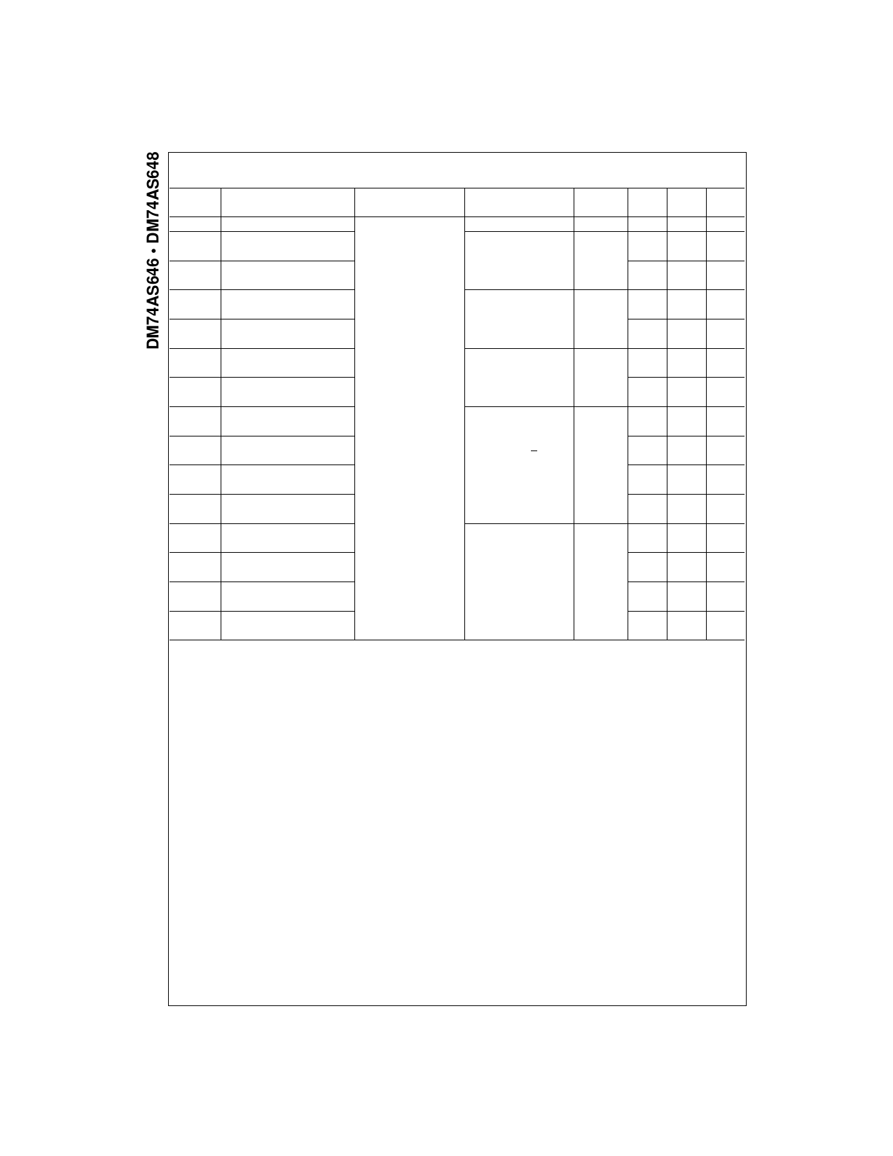
DM74AS648 Switching Characteristics
Symbol
Parameter
Conditions
From
(Input)
To
(Output)
fMAX
tPLH
tPHL
Maximum Clock Frequency
Propagation Delay Time
LOW-to-HIGH Level Output
Propagation Delay Time
HIGH-to-LOW Level Output
VCC = 4.5V to 5.5V,
R1 = R2 = 500Ω
CL = 50 pF
CAB or CBA
A or B
tPLH
Propagation Delay Time
LOW-to-HIGH Level Output
tPHL
Propagation Delay Time
HIGH-to-LOW Level Output
A or B
B or A
tPLH
Propagation Delay Time
LOW-to-HIGH Level Output
tPHL
Propagation Delay Time
HIGH-to-LOW Level Output
SBA or SAB
(Note 7)
A or B
tPZH
Output Enable Time
to HIGH Level Output
tPZL
Output Enable Time
to LOW Level Output
tPHZ
Output Disable Time
from HIGH Level Output
Enable G
A or B
tPLZ
Output Disable Time
from LOW Level Output
tPZH
Output Enable Time
to HIGH Level Output
tPZL
Output Enable Time
to LOW Level Output
tPHZ
Output Disable Time
from HIGH Level Output
DIR
A or B
tPLZ
Output Disable Time
from LOW Level Output
Note 7: These parameters are measured with the internal output state of the storage register opposite to that of the bus input.
Min
Max
90
2
8.5
2
9
2
8
1
7
2
11
2
9
2
9
3
15
2
9
2
9
3
16
3
18
2
10
2
10
Units
MHz
ns
ns
ns
ns
ns
ns
ns
ns
ns
ns
ns
ns
ns
ns
www.fairchildsemi.com
6
Share Link: 