CY7C63001A Ver la hoja de datos (PDF) - Cypress Semiconductor
Número de pieza
componentes Descripción
fabricante
CY7C63001A Datasheet PDF : 31 Pages
| |||
FOR
FOR
CY7C63000A/CY7C63001A
CY7C63100A/CY7C63101A
XTALOUT
clk1x
(to USB SIE)
clk2x
(to Microcontroller)
Clock
Doubler
30 pF
30 pF
XTALIN
Figure 5-14. Clock Oscillator On-chip Circuit
5.8 Interrupts
Interrupts are generated by the General Purpose I/O lines, the Cext pin, the internal timer, and the USB engine. All interrupts are
maskable by the Global Interrupt Enable Register. Access to this register is accomplished via IORD, IOWR, and IOWX instruc-
tions to address 0x20. Writing a “1” to a bit position enables the interrupt associated with that position. During a reset, the contents
of the Interrupt Enable Register are cleared, disabling all interrupts. Figure 5-15 illustrates the format of the Global Interrupt Enable
Register.
b7
CEXTIE
R/W
b6
GPIOIE
R/W
b5
Reserved
b4
EP1IE
R/W
b3
EP0IE
R/W
b2
1024IE
R/W
b1
128IE
R/W
b0
Reserved
0
0
0
0
0
0
0
0
Figure 5-15. Global Interrupt Enable Register (GIER - Address 0x20)
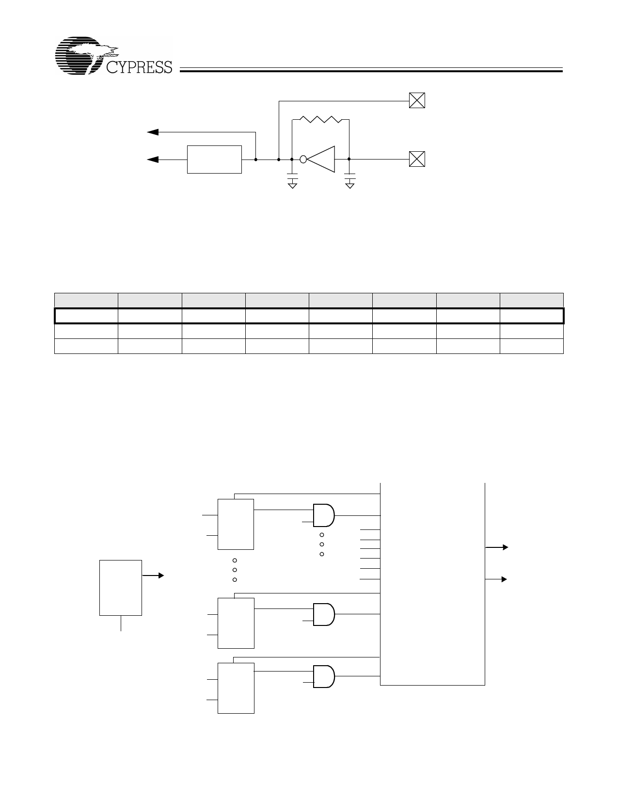
The interrupt controller contains a separate latch for each interrupt. See Figure 5-16 for the logic block diagram for the interrupt
controller. When an interrupt is generated, it is latched as a pending interrupt. It stays as a pending interrupt until it is serviced or
a reset occurs. A pending interrupt only generates an interrupt request if it is enabled in the Global Interrupt Enable Register. The
highest priority interrupt request is serviced following the execution of the current instruction.
When servicing an interrupt, the hardware first disables all interrupts by clearing the Global Interrupt Enable Register. Next, the
interrupt latch of the current interrupt is cleared. This is followed by a CALL instruction to the ROM address associated with the
interrupt being serviced (i.e., the interrupt vector). The instruction in the interrupt table is typically a JMP instruction to the address
of the Interrupt Service Routine (ISR). The user can re-enable interrupts in the interrupt service routine by writing to the appro-
priate bits in the Global Interrupt Enable Register. Interrupts can be nested to a level limited only by the available stack space.
Global
Interrupt
Enable
Register
CLR
Interrupt
Acknowledge
Logic 1
128-ms
Interrupt
CLR
DQ
CLK
Enable [1]
Enable [7:0]
Logic 1
GPIO
Interrupt
CLR
DQ
CLK
Enable [6]
CLR
Logic 1 D
Q Enable [7]
CEXT
CLK
128-ms CLR
128-ms IRQ
1-ms CLR
1-ms IRQ
End P0 CLR
End P0 IRQ
End P1 CLR
End P1 IRQ
GPIO CLR
GPIO IRQ
IRQ
Interrupt
Vector
Wake-up CLR
Wake-up IRQ
Interrupt
Priority
Encoder
Figure 5-16. Interrupt Controller Logic Block Diagram
Document #: 38-08026 Rev. **
Page 14 of 31
Share Link: 