BD8961NV-E2 Ver la hoja de datos (PDF) - ROHM Semiconductor
Número de pieza
componentes Descripción
fabricante
BD8961NV-E2
ROHM Semiconductor
BD8961NV-E2 Datasheet PDF : 14 Pages
| |||
BD8961NV
Technical Note
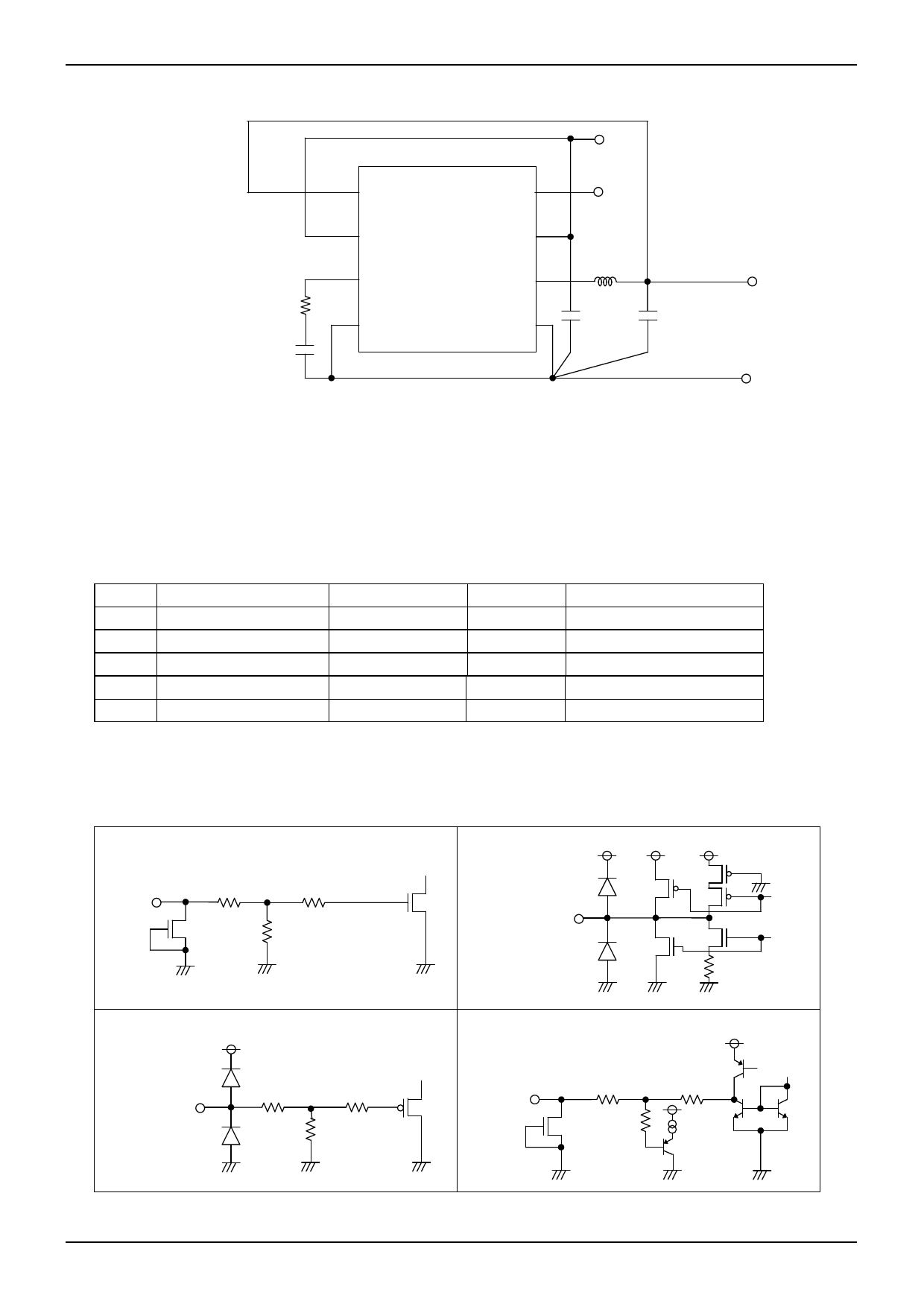
●BD8961NV Cautions on PC Board layout
VCC
RITH
③
CITH
1 VOUT
2
VCC
3 ITH
4
GND
EN 8
EN
7
PVCC
SW 6
L
5
CIN
Co
PGND
②
①
VOUT
Fig.32 Layout diagram
GND
① For the sections drawn with heavy line, use thick conductor pattern as short as possible.
② Lay out the input ceramic capacitor CIN closer to the pins PVCC and PGND, and the output capacitor Co closer to
the pin PGND.
③ Lay out CITH and RITH between the pins ITH and GND as near as possible with least necessary wiring.
※ SON008V5060 (BD8961NV) has thermal FIN on the reverse of the package.
The package thermal performance may be enhanced by bonding the FIN to GND plane which take a large area of PCB.
●Recommended components Lists on above application
Symbol
Part
Value
Manufacturer
Series
L Coil
2.2uH
TDK
LTF5022-2R2N3R2
CIN Ceramic capacitor
22uF
Kyocera
CM32X5R226M10A
CO Ceramic capacitor
22uF
Kyocera
CM316B226M06A
CITH Ceramic capacitor
680pF
murata
GRM18 Serise
RITH Resistance
12kΩ
Rohm
MCR03Serise
*The parts list presented above is an example of recommended parts. Although the parts are sound, actual circuit characteristics should be checked on your
application carefully before use. Be sure to allow sufficient margins to accommodate variations between external devices and this IC when employing the
depicted circuit with other circuit constants modified. Both static and transient characteristics should be considered in establishing these margins. When
switching noise is substantial and may impact the system, a low pass filter should be inserted between the VCC and PVCC pins, and a schottky barrier diode
established between the SW and PGND pins.
●I/O equivalence circuit
・EN pin
・SW pin
PVCC PVCC
PVCC
EN
SW
・VOUT pin
VCC
VOUT
10kΩ
・ITH pin
ITH
www.rohm.com
© 2010 ROHM Co., Ltd. All rights reserved.
Fig.33 I/O equivalence circuit
11/13
VCC
2010.04 - Rev.B
Share Link: 