MCM6343YJ Ver la hoja de datos (PDF) - Motorola => Freescale
Número de pieza
componentes Descripción
fabricante
MCM6343YJ Datasheet PDF : 10 Pages
| |||
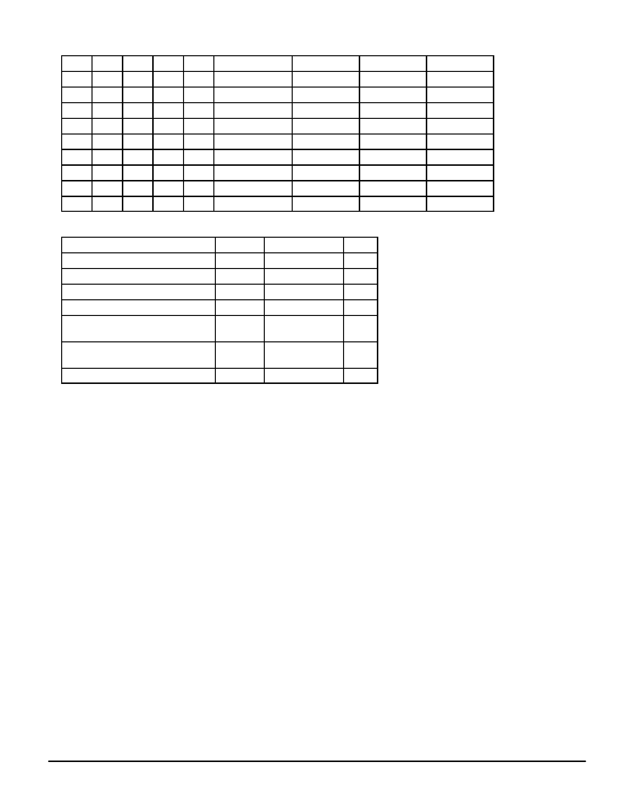
TRUTH TABLE (X = Don’t Care)
E
G
W
LB UB
H
X
X
X
X
L
H
H
X
X
L
X
X
H
H
L
L
H
L
H
L
L
H
H
L
L
L
H
L
L
L
X
L
L
H
L
X
L
H
L
L
X
L
L
L
Mode
Not Selected
Output Disabled
Output Disabled
Low Byte Read
High Byte Read
Word Read
Low Byte Write
High Byte Write
Word Write
VDD Current
ISB1, ISB2
IDDA
IDDA
IDDA
IDDA
IDDA
IDDA
IDDA
IDDA
DQ0 – DQ7
High–Z
High–Z
High–Z
Dout
High–Z
Dout
Din
High–Z
Din
DQ8 – DQ15
High–Z
High–Z
High–Z
High–Z
Dout
Dout
High–Z
Din
Din
ABSOLUTE MAXIMUM RATINGS (See Notes)
Rating
Symbol
Value
Unit
Supply Voltage
Voltage on Any Pin
Output Current per Pin
Package Power Dissipation
Temperature Under Bias Commercial
Industrial
VDD
Vin
Iout
PD
Tbias
– 0.5 to + 4.6
V
– 0.5 to VDD + 0.5
V
± 20
mA
TBD
W
– 10 to + 85
°C
– 45 to + 90
Operating Temperature Commercial
TA
Industrial
0 to + 70
°C
– 45 to + 85
Storage Temperature
Tstg
– 55 to + 150
°C
NOTES:
1. Permanent device damage may occur if ABSOLUTE MAXIMUM RATINGS are
exceeded. Functional operation should be restricted to RECOMMENDED OPER-
ATING CONDITIONS. Exposure to higher than recommended voltages for extended
periods of time could affect device reliability.
2. All voltages are referenced to VSS.
3. Power dissipation capability will be dependent upon package characteristics and use
environment.
This device contains circuitry to protect the
inputs against damage due to high static volt-
ages or electric fields; however, it is advised
that normal precautions be taken to avoid ap-
plication of any voltage higher than maximum
rated voltages to these high–impedance circuits.
This CMOS memory circuit has been
designed to meet the dc and ac specifications
shown in the tables, after thermal equilibrium
has been established. The circuit is in a test
socket or mounted on a printed circuit board and
transverse air flow of at least 500 linear feet per
minute is maintained.
MCM6343
2
MOTOROLA FAST SRAM
Share Link: 