ADUM7442ARQZ-RL7 Ver la hoja de datos (PDF) - Analog Devices
Número de pieza
componentes Descripción
fabricante
ADUM7442ARQZ-RL7 Datasheet PDF : 20 Pages
| |||
ADuM7440/ADuM7441/ADuM7442
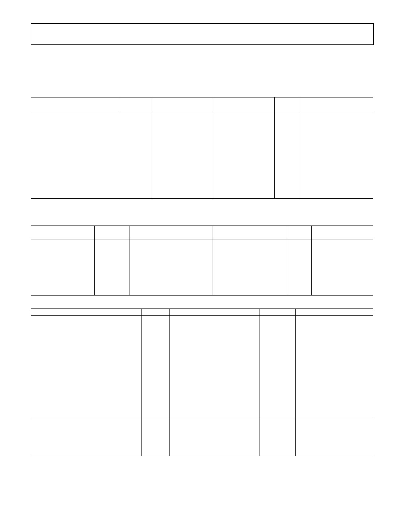
ELECTRICAL CHARACTERISTICS—MIXED 5 V/3.3 V OPERATION
All typical specifications are at TA = 25°C, VDD1 = 5 V, VDD2 = 3.3 V. Minimum/maximum specifications apply over the entire recom-
mended operation range of 4.5 V ≤ VDD1 ≤ 5.5 V, 3.0 V ≤ VDD2 ≤ 3.6 V; and −40°C ≤ TA ≤ +105°C, unless otherwise noted. Switching
specifications are tested with CL = 15 pF and CMOS signal levels, unless otherwise noted.
Table 7.
Parameter
SWITCHING SPECIFICATIONS
Data Rate
Propagation Delay
Pulse Width Distortion
Change vs. Temperature
Pulse Width
Propagation Delay Skew1
Channel Matching
Codirectional
Opposing-Direction
Jitter
Symbol
A Grade
C Grade
Min Typ Max Min Typ Max Unit
Test Conditions
1
25
Mbps Within PWD limit
tPHL tPLH
55 80
30 42 55
ns
50% input to 50% output
PWD
10 25
2
5
ns
|tPLH − tPHL|
5
3
ps/°C
PW
250
40
ns
Within PWD limit
tPSK
20
10
ns
tPSKCD
tPSKOD
25
30
2
2
5
ns
3
6
ns
2
ns
1 tPSK is the magnitude of the worst-case difference in tPHL or tPLH that is measured between units at the same operating temperature, supply voltages, and output load
within the recommended operating conditions.
Table 8.
Parameter
SUPPLY CURRENT
ADuM7440
ADuM7441
ADuM7442
Symbol
IDD1
IDD2
IDD1
IDD2
IDD1
IDD2
1 Mbps—A, C Grades
Min
Typ
Max
4.4
5.5
1.6
2.1
3.7
5.0
2.2
2.8
3.2
3.9
2.0
2.6
25 Mbps—C Grade
Min
Typ Max
28
35
3.5
4.5
19
27
5.2
7.0
15
20
7.8
12
Unit
mA
mA
mA
mA
mA
mA
Test Conditions
Table 9. For All Models
Parameter
DC SPECIFICATIONS
Logic High Input Threshold
Logic Low Input Threshold
Logic High Output Voltages
Logic Low Output Voltages
Input Current per Channel
Supply Current per Channel
Quiescent Input Supply Current
Quiescent Output Supply Current
Dynamic Input Supply Current
Dynamic Output Supply Current
AC SPECIFICATIONS
Output Rise/Fall Time
Common-Mode Transient Immunity1
Refresh Rate
Symbol Min
Typ
Max
Unit
Test Conditions
VIH
0.7 VDDx
V
VIL
0.3 VDDx V
VOH
VDDx − 0.1
VDDx
V
VDDx− 0.4
VDDx − 0.2
V
VOL
0.0
0.1
V
0.2
0.4
V
II
−10
+0.01
+10
µA
IOx = −20 µA, VIx = VIxH
IOx = −4 mA, VIx = VIxH
IOx = 20 µA, VIx = VIxL
IOx = 4 mA, VIx = VIxL
0 V ≤ VIx ≤ VDDx
IDDI(Q)
IDDO(Q)
IDDI(D)
IDDO(D)
0.77
0.40
0.26
0.02
mA
mA
mA/Mbps
mA/Mbps
tR/tF
2.5
|CM|
15
20
fr
1.2
ns
kV/µs
Mbps
10% to 90%
VIx = VDDx, VCM = 1000 V,
transient magnitude = 800 V
1 |CM| is the maximum common-mode voltage slew rate that can be sustained while maintaining VO > 0.8 VDD. The common-mode voltage slew rates apply to both
rising and falling common-mode voltage edges.
Rev. B | Page 5 of 20
Share Link: 