ADUM1250WSRZ-RL7(RevC) Ver la hoja de datos (PDF) - Analog Devices
Número de pieza
componentes Descripción
fabricante
ADUM1250WSRZ-RL7 Datasheet PDF : 12 Pages
| |||
ADuM1250/ADuM1251
APPLICATIONS INFORMATION
FUNCTIONAL DESCRIPTION
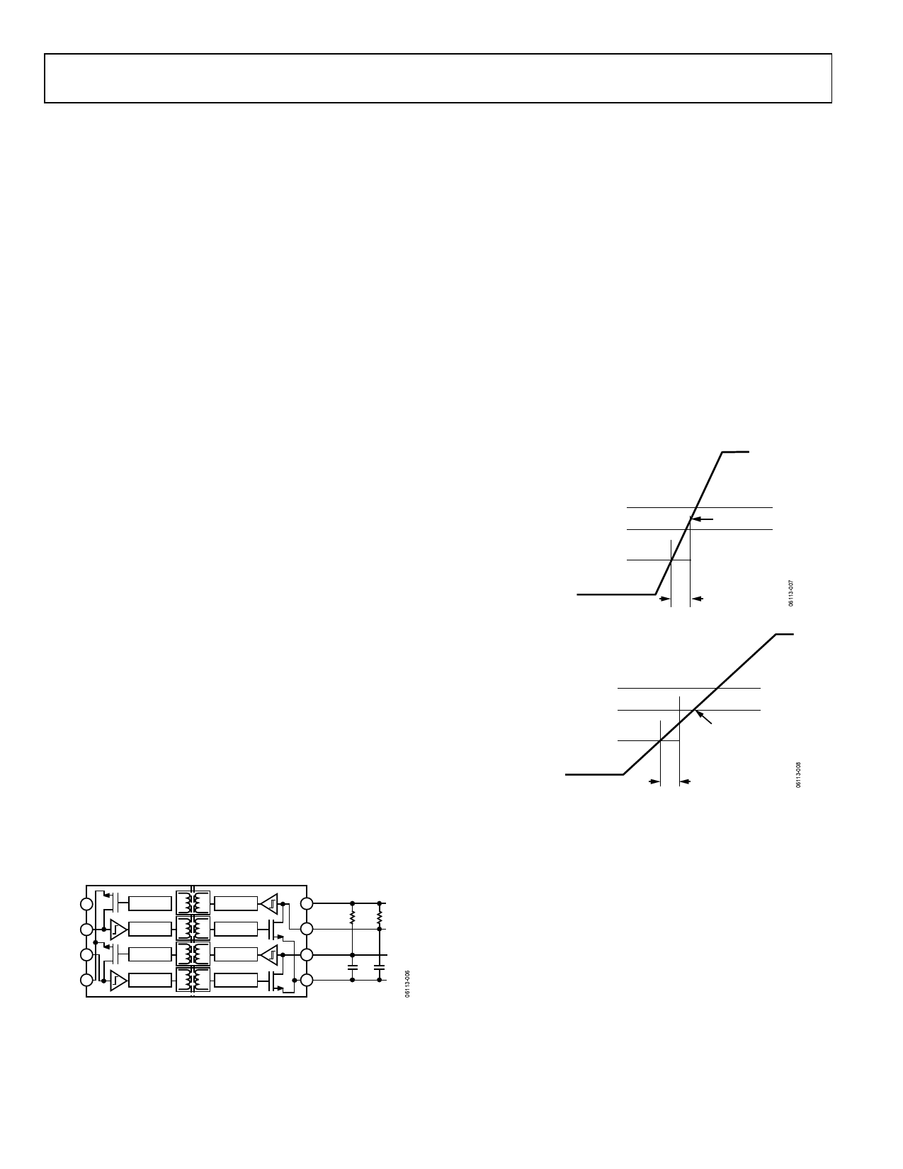
The ADuM1250/ADuM1251 interfaces on each side to a
bidirectional I2C signal. Internally, the I2C interface is split
into two unidirectional channels communicating in opposing
directions via a dedicated iCoupler isolation channel for each.
One channel (the bottom channel of each channel pair shown
in Figure 6) senses the voltage state of the Side 1 I2C pin and
transmits its state to its respective Side 2 I2C pin.
Both the Side 1 and the Side 2 I2C pins are designed to interface
to an I2C bus operating in the 3.0 V to 5.5 V range. A logic low
on either causes the opposite pin to be pulled low enough to
comply with the logic low threshold requirements of other I2C
devices on the bus. Avoidance of I2C bus contention is ensured
by an input low threshold at SDA1 or SCL1 guaranteed to be at
least 50 mV less than the output low signal at the same pin. This
prevents an output logic low at Side 1 being transmitted back to
Side 2 and pulling down the I2C bus.
Since the Side 2 logic levels/thresholds are standard I2C values,
multiple ADuM1250/ADuM1251 devices connected to a bus by
their Side 2 pins can communicate with each other and with other
devices having I2C compatibility. A distinction is made between
I2C compatibility and I2C compliance. I2C compatibility refers to
situations in which a component's logic levels do not necessarily
meet the requirements of the I2C specification but still allow the
component to communication with an I2C-compliant device.
I2C compliance refers to situations in which a component's logic
levels meet the requirements of the I2C specification.
However, since the Side 1 pin has a modified output level/input
threshold, this side of the ADuM1250/ADuM1251 can only
communicate with devices conforming to the I2C standard. In
other words, Side 2 of the ADuM1250/ADuM1251 is I2C-compliant,
while Side 1 is only I2C-compatible.
The output logic low levels are independent of the VDD1 and
VDD2 voltages. The input logic low threshold at Side 1 is also
independent of VDD1. However, the input logic low threshold at
Side 2 is designed to be at 0.3 VDD2, consistent with I2C require-
ments. The Side 1 and Side 2 pins have open-collector outputs
whose high levels are set via pull-up resistors to their respective
supply voltages.
VDD1 1
SDA1 2
SCL1 3
GND1 4
DECODE
ENCODE
DECODE
ENCODE
ENCODE
DECODE
ENCODE
DECODE
VDD2
8
SDA2
7
SCL2
6
GND2
5
R2 R2
CL CL
Figure 6. ADuM1250 Block Diagram
STARTUP
Both the VDD1 and VDD2 supplies have an undervoltage lockout
feature to prevent the signal channels from operating unless
certain criteria are met. This avoids the possibility of input logic
low signals from pulling down the I2C bus inadvertently during
power-up/power-down.
The two criteria that must be met in order for the signal
channels to be enabled are as follows:
• Both supplies must be at least 2.5 V.
• At least 40 μs must elapse after both supplies exceed the
internal startup threshold of 2.0 V.
Until both of these criteria are met for both supplies, the
ADuM1250/ADuM1251 outputs are pulled high, ensuring a
startup that avoids any disturbances on the bus. Figure 7 and
Figure 8 illustrate the supply conditions for fast and slow input
supply slew rates.
MINIMUM RECOMMENDED
OPERATING SUPPLY, 3.0V
MINIMUM VALID SUPPLY, 2.5V
INTERNAL STARTUP
THRESHOLD, 2.0V
SUPPLY VALID
40µs
Figure 7. Start-Up Condition, Supply Slew Rate > 12.5 V/ms
MIN. RECOMMENDED
OPERATING SUPPLY, 3.0V
MIN. VALID SUPPLY, 2.5V
INTERNAL STARTUP
THRESHOLD, 2.0V
SUPPLY VALID
40µs
Figure 8. Start-Up Condition, Supply Slew Rate < 12.5 V/ms
Rev. C | Page 10 of 12
Share Link: 