ADT7517ARQ Ver la hoja de datos (PDF) - Analog Devices
Número de pieza
componentes Descripción
fabricante
ADT7517ARQ
Analog Devices
ADT7517ARQ Datasheet PDF : 44 Pages
| |||
ADT7516/ADT7517/ADT7519
D7 D6 D5 D4 D3 D2 D1 D0
D7 D6 D5 D4 D3 D2 D1 D0
01
01
01
01
01
01
01
01
1 Default settings at power-up.
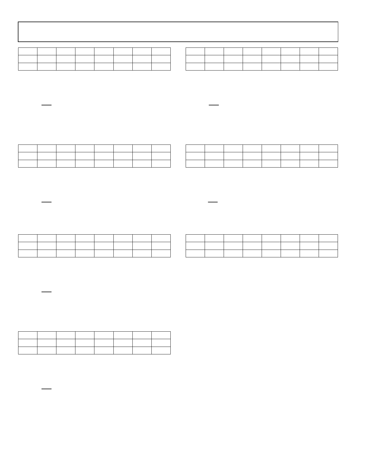
AIN2 VHIGH Limit Register (Read/Write) [Address = 0x2B]
This limit register is an 8-bit read/write register that stores the
AIN2 input upper limit, and causes an interrupt and activates
the INT/INT output (if enabled). For this to happen, the
measured AIN2 value has to be greater than the value in this
register. Because it is an 8-bit register, the resolution is four
times less than the resolution of the 10-bit ADC. The default
value is full-scale voltage.
D7 D6 D5 D4 D3 D2 D1 D0
D7 D6 D5 D4 D3 D2 D1 D0
11
11
11
11
11
11
11
11
1 Default settings at power-up.
AIN2 VLOW Limit Register (Read/Write) [Address = 0x2C]
This limit register is an 8-bit read/write register that stores the
AIN2 input lower limit, and causes an interrupt and activates
the INT/INT output (if enabled). For this to happen, the meas-
ured AIN2 value has to be less than or equal to the value in this
register. Because it is an 8-bit register, the resolution is four times
less than the resolution of the 10-bit ADC. The default value is 0 V.
D7 D6 D5 D4 D3 D2 D1 D0
D7 D6 D5 D4 D3 D2 D1 D0
01
01
01
01
01
01
01
01
1 Default settings at power-up.1 Default settings at power-up.
AIN3 VHIGH Limit Register (Read/Write) [Address = 0x2D]
This limit register is an 8-bit read/write register that stores the
AIN3 input upper limit, and causes an interrupt and activates
the INT/INT output (if enabled). For this to happen, the
measured AIN3 value has to be greater than the value in this
register. Because it is an 8-bit register, the resolution is four
times less than the resolution of the 10-bit ADC. The default
value is full-scale voltage.
D7 D6 D5 D4 D3 D2 D1 D0
D7 D6 D5 D4 D3 D2 D1 D0
11
11
11
11
11
11
11
11
1 Default settings at power-up.
AIN3 VLOW Limit Register (Read/Write) [Address = 0x2E]
This limit register is an 8-bit read/write register that stores the
AIN3 input lower limit, and causes an interrupt and activates
the INT/INT output (if enabled). For this to happen, the meas-
ured AIN3 value has to be less than or equal to the value in this
register. Because it is an 8-bit register, the resolution is four times
less than the resolution of the 10-bit ADC. The default value is 0 V.
D7 D6 D5 D4 D3 D2 D1 D0
D7 D6 D5 D4 D3 D2 D1 D0
01
01
01
01
01
01
01
01
1 Default settings at power-up.
AIN4 VHIGH Limit Register (Read/Write) [Address = 0x2F]
This limit register is an 8-bit read/write register that stores the
AIN4 input upper limit, and causes an interrupt and activates
the INT/INT output (if enabled). For this to happen, the
measured AIN4 value has to be greater than the value in this
register. Because it is an 8-bit register, the resolution is four
times less than the resolution of the 10-bit ADC. The default
value is full-scale voltage.
D7 D6 D5 D4 D3 D2 D1 D0
D7 D6 D5 D4 D3 D2 D1 D0
11
11
11
11
11
11
11
11
1 Default settings at power-up.
AIN4 VLOW Limit Register (Read/Write) [Address = 0x30]
This limit register is an 8-bit read/write register that stores the
AIN4 input lower limit, and causes an interrupt and activates
the INT/INT output (if enabled). For this to happen, the measured
AIN4 value has to be less than or equal to the value in this register.
Because it is an 8-bit register, the resolution is four times less
than the resolution of the 10-bit ADC. The default value is 0 V.
D7 D6 D5 D4 D3 D2 D1 D0
D7 D6 D5 D4 D3 D2 D1 D0
01
01
01
01
01
01
01
01
1 Default settings at power-up.
Device ID Register (Read-Only) [Address = 0x4D]
This 8-bit read-only register indicates the part model of the
device: ADT7516 = 0x03, ADT7517 = 0x07, and ADT7519 = 0x0B.
Manufacturer’s ID Register (Read-Only) [Address = 0x4E]
This register contains the manufacturer’s identification number.
ID number of Analog Devices, Inc. is 0x41.
Silicon Revision Register (Read-Only) [Address = 0x4F]
This register is divided into the four LSBs representing the
stepping and the four MSBs representing the version. The
stepping contains the manufacturer’s code for minor revisions
or steppings to the silicon. The version is the ADT7516/
ADT7517/ADT7519 version number.
SPI Lock Status Register (Read-Only) [Address = 0x7F]
Bit D0 (LSB) of this read-only register indicates whether or not
the SPI interface is locked. Writing to this register causes the
device to malfunction. The default value is 0x00.
0 = I2C interface.
1 = SPI interface selected and locked.
Rev. B | Page 36 of 44
Share Link: 