ADT75ARZ Ver la hoja de datos (PDF) - Analog Devices
Número de pieza
componentes Descripción
fabricante
ADT75ARZ Datasheet PDF : 24 Pages
| |||
ADT75
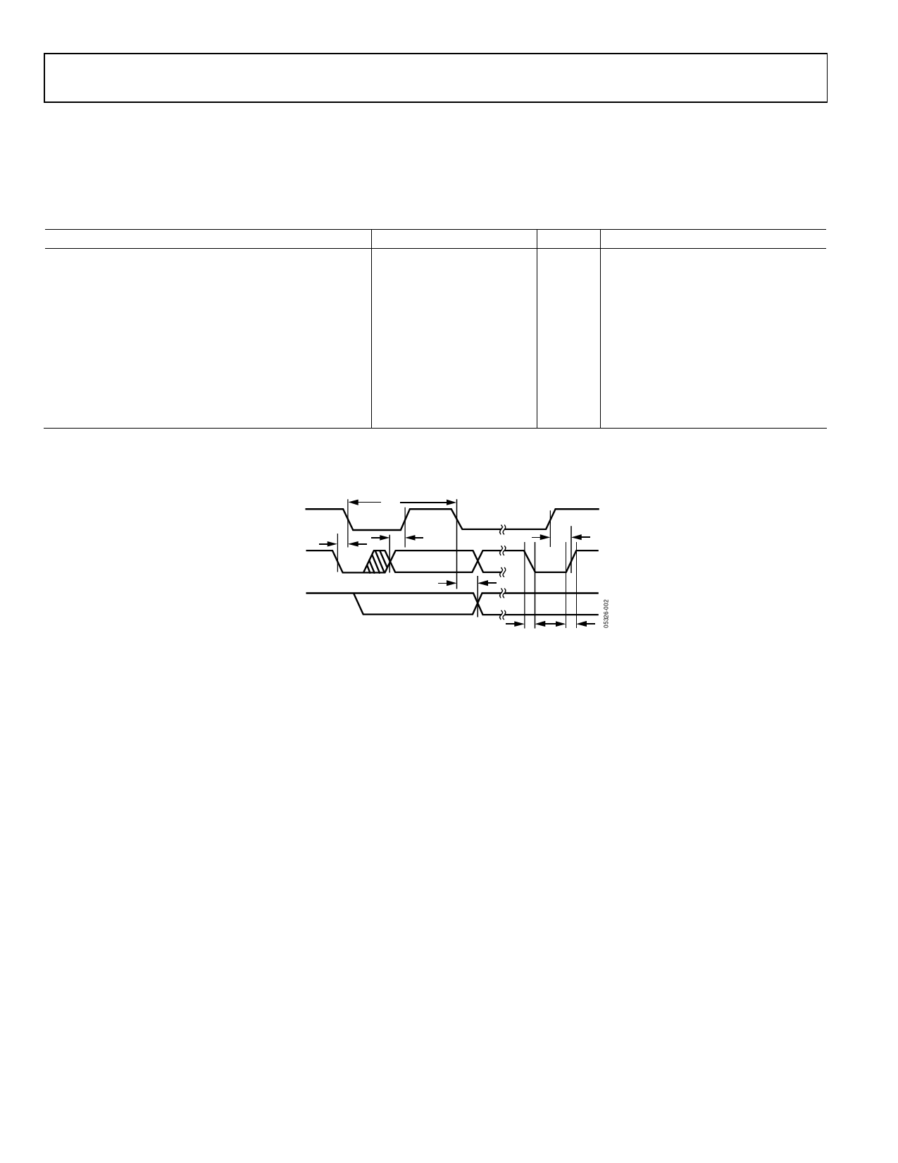
TIMING SPECIFICATIONS AND DIAGRAM
Measure the SDA and SCL timing with the input filters turned on to meet the fast mode I2C specification. Switching off the input filters
improves the transfer rate but has a negative affect on the EMC behavior of the part.
TA = TMIN to TMAX, VDD = +2.7 V to +5.5 V, unless otherwise noted.
Table 3.
Parameter1
MIN TYP MAX
Serial Clock Period, t1
2.5
Data In Setup Time to SCL High, t2
Data Out Stable After SCL Low, t3
Data Out Stable After SCL Low, t3
50
0
0.92
0
3.452
SDA Low Setup Time to SCL Low (Start Condition), t4
50
SDA High Hold Time After SCL High (Stop Condition), t5 50
SDA and SCL Rise Time, t6
300
SDA and SCL Rise Time, t6
1000
SDA and SCL Fall Time, t7
300
Capacitive Load for each Bus Line, CB
400
1 Guaranteed by design and characterization; not production tested.
2 This time has to be met only if the master does not stretch the low period of the SCL signal.
Units
μs
ns
ns
μs
ns
ns
ns
ns
ns
pF
Comments
Fast mode I2C. See Figure 2
See Figure 2
Fast mode I2C. See Figure 2
Standard mode I2C. See Figure 2
See Figure 2
See Figure 2
Fast mode I2C. See Figure 2
Standard mode I2C. See Figure 2
See Figure 2
SCL
SDA
DATA IN
SDA
DATA OUT
t1
t4
t2
t5
t3
t7
t6
Figure 2. SMBus/I2C Timing Diagram
Rev. 0 | Page 6 of 24
Share Link: 