ADP5033 Ver la hoja de datos (PDF) - Analog Devices
Número de pieza
componentes Descripción
fabricante
ADP5033 Datasheet PDF : 28 Pages
| |||
ADP5033
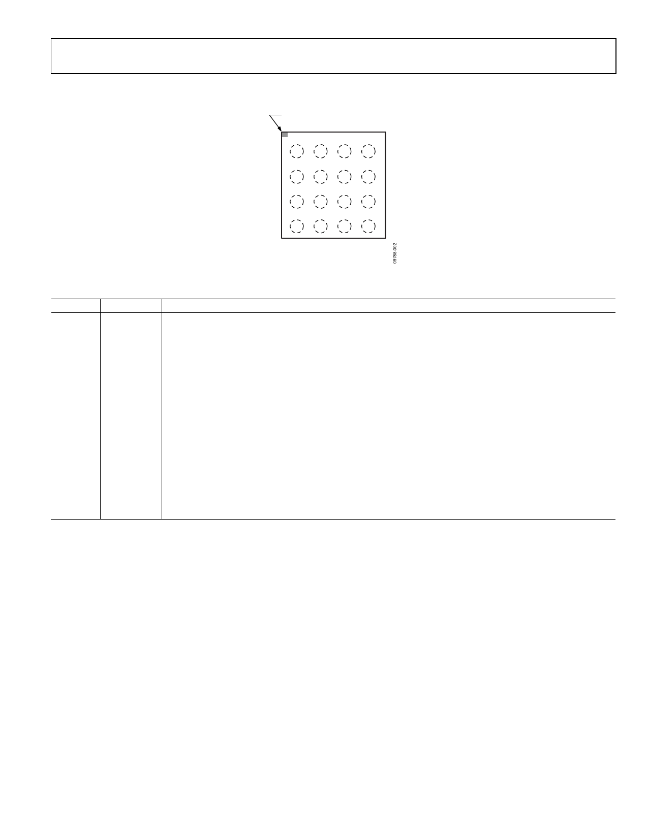
PIN CONFIGURATION AND FUNCTION DESCRIPTIONS
BALL A1
INDICATOR
1
2
VOUT3 VIN3
A
3
4
VIN4 VOUT4
AGND MODE ENA ENB
B
VIN1 VOUT1 VOUT2 VIN2
C
PGND1 SW1 SW2 PGND2
D
TOP VIEW
(BALL SIDE DOWN)
Not to Scale
Figure 2. Pin Configuration—View from the Top of the Die
Table 7. Pin Function Descriptions
Pin No. Mnemonic Description
A1
VOUT3
LDO1 Output Voltage and Sensing Input.
A2
VIN3
LDO1 Input Supply (1.7 V to 5.5 V, VIN4 ≤ VIN1 = VIN2).
A3
VIN4
LDO2 Input Supply (1.7 V to 5.5 V, VIN3 ≤ VIN1 = VIN2).
A3
VOUT4
LDO2 Output Voltage and Sensing Input.
B1
AGND
Analog Ground.
B2
MODE
BUCK1/BUCK2 Operating Mode. MODE = high: forced PWM operation. MODE = low: auto PWM/PSM operation.
B3
ENA
Regulator Enable Pin A, Active High. The regulators turned on with ENA are factory programmed.
B4
ENB
Regulator Enable Pin B, Active High. The regulators turned on with ENB are factory programmed.
C1
VIN1
BUCK1 Input Supply (2.3 V to 5.5 V) and UVLO Detection. Connect VIN1 to VIN2.
C2
VOUT1
BUCK1 Output Voltage Sensing Input.
C3
VOUT2
BUCK2 Output Voltage Sensing Input.
C4
VIN2
BUCK2 Input Supply (2.3 V to 5.5 V). Connect VIN2 to VIN1.
D1
PGND1
Dedicated Power Ground for BUCK1.
D2
SW1
BUCK1 Switching Node.
D3
SW2
BUCK2 Switching Node.
D4
PGND2
Dedicated Power Ground for BUCK2.
Rev. 0 | Page 7 of 28
Share Link: 