AD8244ARMZ Ver la hoja de datos (PDF) - Analog Devices
Número de pieza
componentes Descripción
fabricante
AD8244ARMZ Datasheet PDF : 20 Pages
| |||
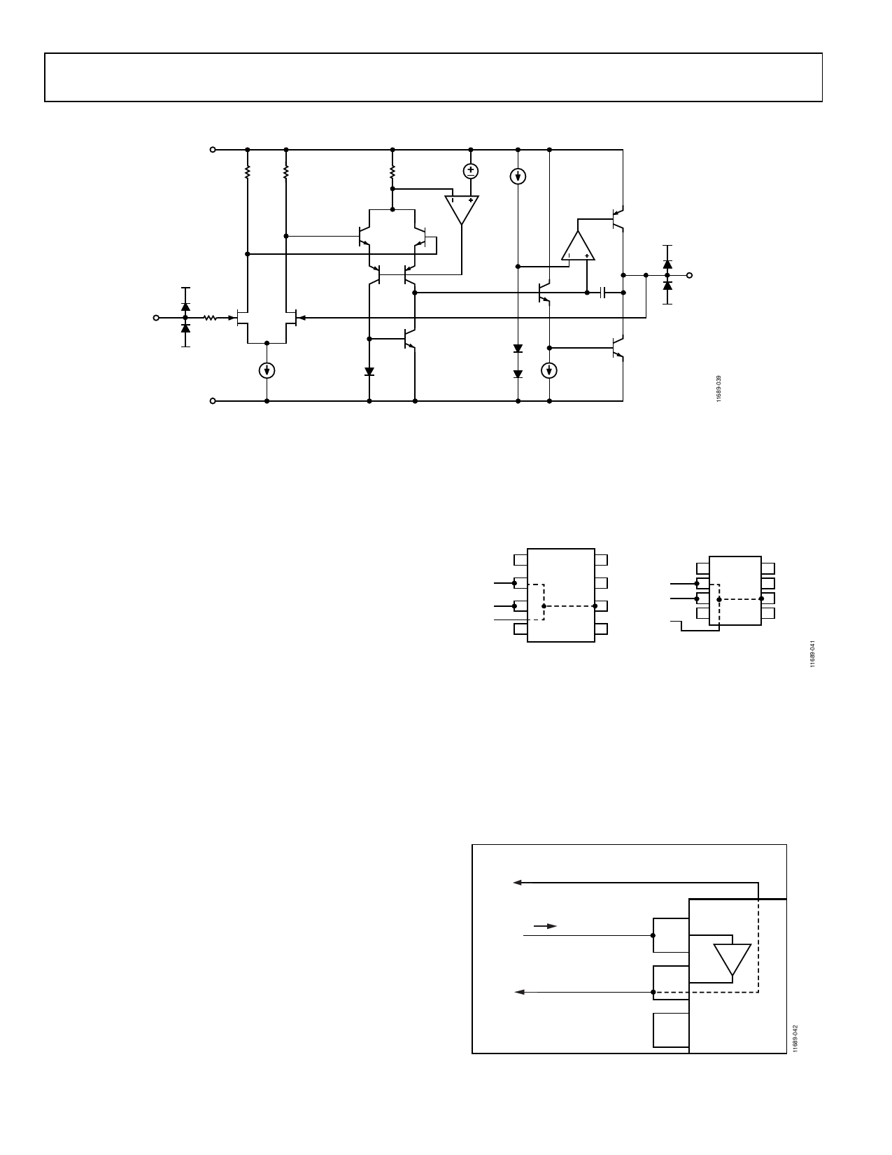
AD8244
THEORY OF OPERATION
+VS
Data Sheet
+VS
500Ω
IN
–VS
+VS
OUT
–VS
–VS
OVERVIEW
Figure 38. Simplified Schematic
of these op amps is to route the guard trace between the input
The AD8244 is a precision, quad, FET input, unity-gain buffer
that is designed to isolate very large source impedances from
the rest of the signal chain. N-channel JFETs are used as the
input transistors to provide a low offset (350 µV maximum),
low noise (13 nV/√Hz typical), high impedance (more than
10 TΩ) input stage that operates right down to the negative supply
voltage. Using a new drift trimming method, the B grade AD8244
is able to achieve very low offset voltage over temperature
(0.545 mV maximum), and it introduces minimal system error
over temperature. The AD8244 design is optimized for high
precision applications, such as buffers for biopotential electrodes,
where it is important that buffers have very high impedance
inputs and channels that match closely. Because the AD8244
fits into a 10-lead package, whereas a quad op amp requires a
minimum of 14 leads, routing space is reduced and parasitics
from the feedback traces are eliminated. Furthermore, the
flexible design and the high channel density of the AD8244
allow it to be used in the signal chain anywhere a unity-gain
buffer is needed.
GUARDING
pin and the supply pin. Traces can be routed between pins for
large packages, such as DIP or even SOIC; however, the board
area consumed by these packages is prohibitive for many
modern applications.
LARGE FOOTPRINT
PACKAGES
SMALL FOOTPRINT
PACKAGES
1
GUARD –IN 2
INPUT +IN 3
GUARD
–VS 4
SINGLE
OP AMP
8
7 +VS GUARD
INPUT
6 OUT
GUARD
5
1
–IN 2
+IN
3
–VS 4
SINGLE
OP AMP
8
7 +VS
6 OUT
5
*LEAKAGE PATH FROM +IN TO –VS
CAUSES LARGE INPUT CURRENT
Figure 39. Single Op Amp Guarding Patterns
The AD8244 solves this problem with a unique pinout that
naturally isolates the high impedance inputs from the low
impedance nodes, such as the supplies and outputs of the other
buffers. Additionally, the buffers of the AD8244 can be used to
guard their own inputs, reducing the voltage gradient seen by the
input to only the low offset voltage of the buffer. The AD8244
facilitates this by making guard traces easy to route without the
When using low input bias current FET input amplifiers,
need for traces to go between pins.
designers must pay careful attention to voltage gradients from
the input node to adjacent conductors on the board. These
gradients can create leakage currents that overwhelm the input
GUARD TRACE SURROUNDS INPUT NODE
impedance and bias current performance of the FET input.
These leakage currents get much worse with contamination,
humidity, and temperature. Guarding techniques can be used to
FROM SENSOR
IN A
IN A
1
protect against parasitic leakage currents by greatly reducing the
voltage gradient seen by the input node. Physically, a guard is a
low impedance conductor that surrounds a high impedance
node and is raised to the voltage of that node. It serves to buffer
GUARD TRACE
OUT A
SOLDER MASK REMOVED
OUT A
2
AD8244
leakage by diverting it away from the sensitive node and into
the low impedance guard. A complication results from the fact
3 +VS
that many traditional op amp pinouts place a supply pin next to
the noninverting input. The only way to guard the input of one
Figure 40. Guarding with the AD8244
Rev. 0 | Page 14 of 20
Share Link: 