AD7921 Ver la hoja de datos (PDF) - Analog Devices
Número de pieza
componentes Descripción
fabricante
AD7921 Datasheet PDF : 28 Pages
| |||
AD7911/AD7921
TYPICAL CONNECTION DIAGRAM
Figure 22 shows a typical connection diagram for the AD7911/
AD7921. VREF is taken internally from VDD and as such VDD
should be well decoupled. This provides an analog input range
of 0 V to VDD. The conversion result is output in a 16-bit word
with two leading zeros, followed by the channel identifier bit
that identifies the channel converted, followed by an invalid bit
that matches up to the channel converted, followed by the MSB
of the 12-bit or 10-bit result. For the AD7911, the 10-bit result is
followed by two trailing zeros. See the Serial Interface section.
Alternatively, because the supply current required by the
AD7911/AD7921 is so low, a precision reference can be used as
the supply source to the AD7911/AD7921. A REF19x voltage
reference (REF195 for 5 V or REF193 for 3 V) can be used to
supply the required voltage to the ADC (see Figure 22). This
configuration is especially useful, if the power supply is quite
noisy or if the system supply voltages are at some value other
than 5 V or 3 V (for example, 15 V). The REF19x outputs a
steady voltage to the AD7911/AD7921. If the low dropout
REF193 is used, the current it needs to supply to the AD7911/
AD7921 is typically 1.5 mA. When the ADC is converting at a
rate of 250 kSPS, the REF193 needs to supply a maximum of
2 mA to the AD7911/AD7921. The load regulation of the
REF193 is typically 10 ppm/mA (REF193, VS = 5 V), which
results in an error of 20 ppm (60 μV) for the 2 mA drawn from
it. This corresponds to a 0.082 LSB error for the AD7921 with
VDD = 3 V from the REF193 and a 0.061 LSB error for the
AD7911.
For applications where power consumption is a concern, the
power-down mode of the ADC and the sleep mode of the
REF19x reference should be used to improve power perform-
ance. See the Modes of Operation section.
1.5mA 0.1μF
3V
1μF
TANT
REF193
10μF
680nF
VDD
0V TO VDD
INPUT
VIN0
VIN1
GND
AD7911/ SCLK
AD7921 CS
DIN
DOUT
0.1μF
μC/μP
5V
SUPPLY
SERIAL
INTERFACE
Figure 22. REF193 as Power Supply to AD7911/AD7921
Table 6 provides some typical performance data with various
references used as a VDD source and a 50 kHz input tone under
the same setup conditions.
Table 6. AD7921 Performance for Various Voltage
References IC
Reference Tied to VDD
AD7921 SNR Performance (dB)
AD780 at 3 V
−73
REF193
−72.42
ADR433
−72.9
AD780 at 2.5 V
−72.86
REF192
−72.27
ADR421
−72.75
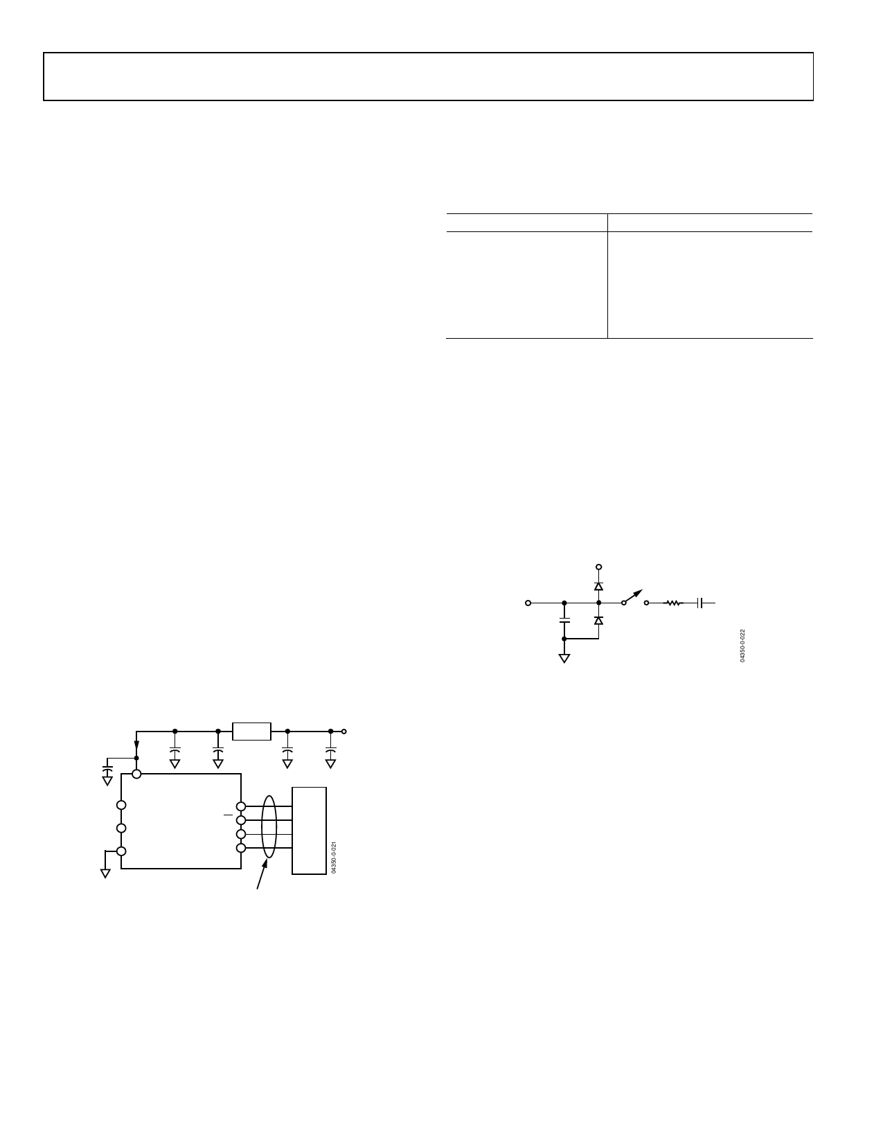
ANALOG INPUT
Figure 23 shows an equivalent circuit of the analog input
structure of the AD7911/AD7921. The two diodes, D1 and D2,
provide ESD protection for the analog input. Care must be
taken to ensure that the analog input signal never exceeds the
supply rails by more than 300 mV, because this would cause
these diodes to become forward biased and start conducting
current into the substrate. The maximum current these diodes
can conduct without causing irreversible damage to the part is
10 mA.
VDD
D1
C2
R1 20pF
VIN
C1
6pF
D2
CONVERSION PHASE—SWITCH OPEN
TRACK PHASE—SWITCH CLOSED
Figure 23. Equivalent Analog Input Circuit
The capacitor C1 in Figure 23 is typically about 6 pF and can
primarily be attributed to pin capacitance. The resistor R1 is a
lumped component made up of the on resistance of a track-
and-hold switch and also includes the on resistance of the input
multiplexer. This resistor is typically about 100 Ω. The capacitor
C2 is the ADC sampling capacitor and has a capacitance of
20 pF typically.
For ac applications, removing high frequency components from
the analog input signal is recommended using a band-pass filter
on the relevant analog input pin. In applications where
harmonic distortion and signal-to-noise ratio are critical, the
analog input should be driven from a low impedance source.
Large source impedances can significantly affect the ac
performance of the ADC. This might necessitate the use of an
input buffer amplifier. The choice of the op amp is a function of
the particular application.
Rev. A | Page 16 of 28
Share Link: 