AD7921ARM-REEL(Rev0) Ver la hoja de datos (PDF) - Analog Devices
Número de pieza
componentes Descripción
fabricante
AD7921ARM-REEL Datasheet PDF : 28 Pages
| |||
AD7911/AD7921
TIMING SPECIFICATIONS
Guaranteed by characterization.
All input signals are specified with tr = tf = 5 ns (10% to 90% of VDD) and timed from a voltage level of 1.6 V.
VDD = 2.35 V to 5.25 V; TA = TMIN to TMAX, unless otherwise noted.
Table 3.
Parameter
fSCLK1
tCONVERT
tQUIET
t1
t2
t33
t43
t5
t6
t74
t8
t9
t105
tPOWER-UP6
Limit at TMIN, TMAX
10
5
16 × tSCLK
14 × tSCLK
30
15
10
30
45
0.4 tSCLK
0.4 tSCLK
10
5
6
30
10
1
Unit
kHz min2
MHz max
ns min
ns min
ns min
ns max
ns max
ns min
ns min
ns min
ns min
ns min
ns max
ns min
µs max
Description
AD7921
AD7911
Minimum quiet time required between bus relinquish and start of next conversion
Minimum CS pulse width
CS to SCLK setup time
Delay from CS until DOUT three-state is disabled
DOUT access time after SCLK falling edge
SCLK low pulse width
SCLK high pulse width
SCLK to DOUT valid hold time
DIN setup time prior to SCLK falling edge
DIN hold time after SCLK falling edge
SCLK falling edge to DOUT three-state
SCLK falling edge to DOUT three-state
Power-up time from full power-down
1 Mark/space ratio for SCLK input is 40/60 to 60/40.
2 Minimum fSCLK at which specifications are guaranteed.
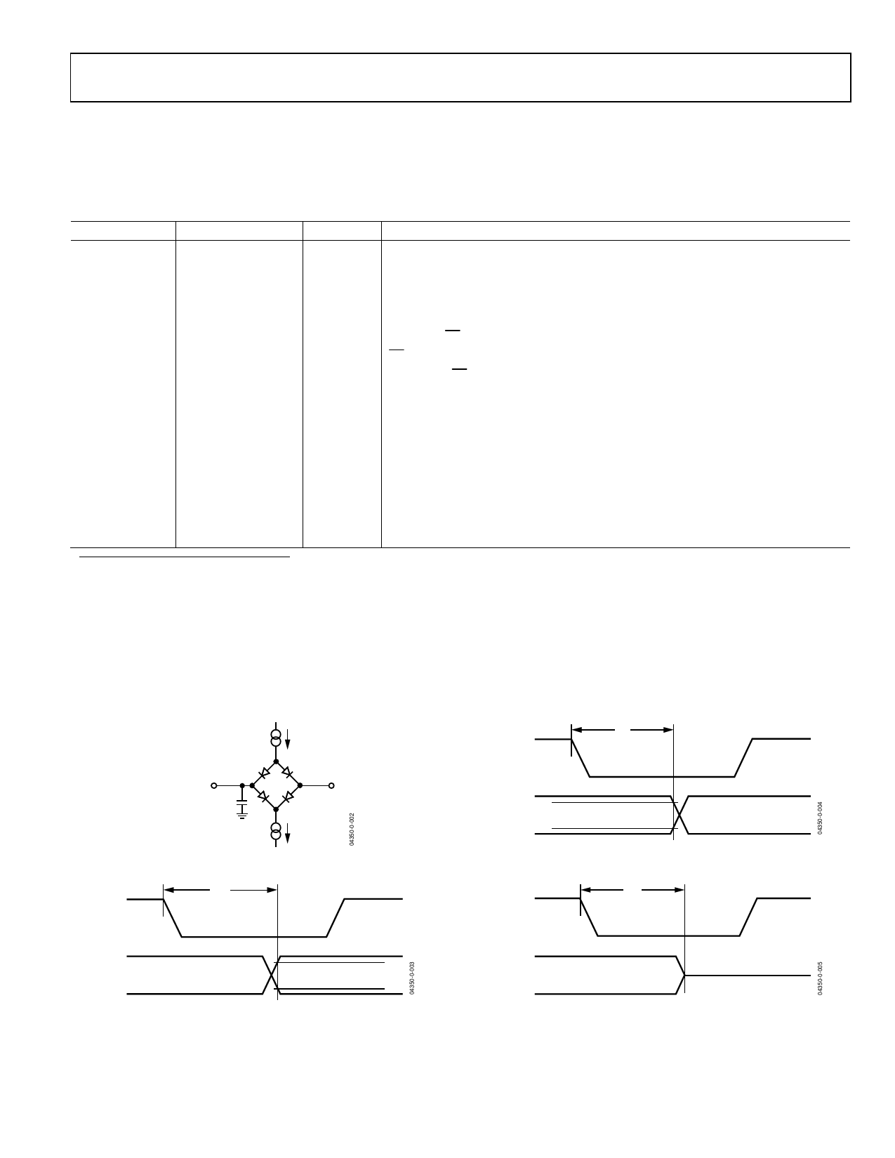
3 Measured with the load circuit in Figure 2 and defined as the time required for the output to cross VIH or VIL voltage.
4 Measured with a 50 pF load capacitor.
5 T10 is derived from the measured time taken by the data outputs to change 0.5 V when loaded with the circuit in Figure 2. The measured number is then extrapolated
back to remove the effects of charging or discharging the 50 pF capacitor. This means that the time, t10, quoted in the timing characteristics is the true bus relinquish
time of the part and is independent of the bus loading.
6 See the Power-Up Time section.
TIMING DIAGRAMS
200µA
IOL
TO OUTPUT
PIN CL
50pF
200µA
IOH
1.6V
Figure 2. Load Circuit for Digital Output Timing Specifications
t4
SCLK
DOUT
VIH
VIL
Figure 3. Access Time after SCLK Falling Edge
t7
SCLK
VIH
DOUT
VIL
SCLK
Figure 4. Hold Time after SCLK Falling Edge
t10
DOUT
1.6V
Figure 5. SCLK Falling Edge to DOUT Three-State
Rev. 0 | Page 7 of 28
Share Link: 