AD7884AN Ver la hoja de datos (PDF) - Analog Devices
Número de pieza
componentes Descripción
fabricante
AD7884AN Datasheet PDF : 16 Pages
| |||
AD7884/AD7885
TIMING CHARACTERISTICS1, 2
(VDD = +5 V ؎ 5%, VSS = –5 V ؎ 5%, AGND = DGND = GND = 0 V. See Figures 2, 3, 4 and 5.)
Parameter
Limit at +25؇C
(All Versions)
Limit at TMIN, TMAX
(A, B Versions)
Units
Conditions/Comments
t1
50
50
t2
100
100
t3
0
0
t4
60
60
t5
0
0
t62
57
57
t73
5
5
50
50
t8
40
40
t9
10
80
t10
25
25
t11
60
60
t12
60
60
t13
55
70
t14
55
70
ns min
ns max
ns min
ns min
ns min
ns max
ns min
ns max
ns min
ns min
ns min
ns min
ns min
ns max
ns max
CONVST Pulse Width
CONVST to BUSY Low Delay
CS to RD Setup Time
RD Pulse Width
CS to RD Hold Time
Data Access Time after RD
Bus Relinquish Time after RD
New Data Valid before Rising Edge of BUSY
HBEN to RD Setup Time
HBEN to RD Hold Time
HBEN Low Pulse Duration
HBEN High Pulse Duration
Propagation Delay from HBEN Falling to Data Valid
Propagation Delay from HBEN Rising to Data Valid
NOTES
1Timing specifications in bold print are 100% production tested. All other times are sample tested at +5 °C to ensure compliance. All input signals are specified
with tr = tf = 5 ns (10% to 90% of 5 V) and timed from a voltage level of 1.6 V.
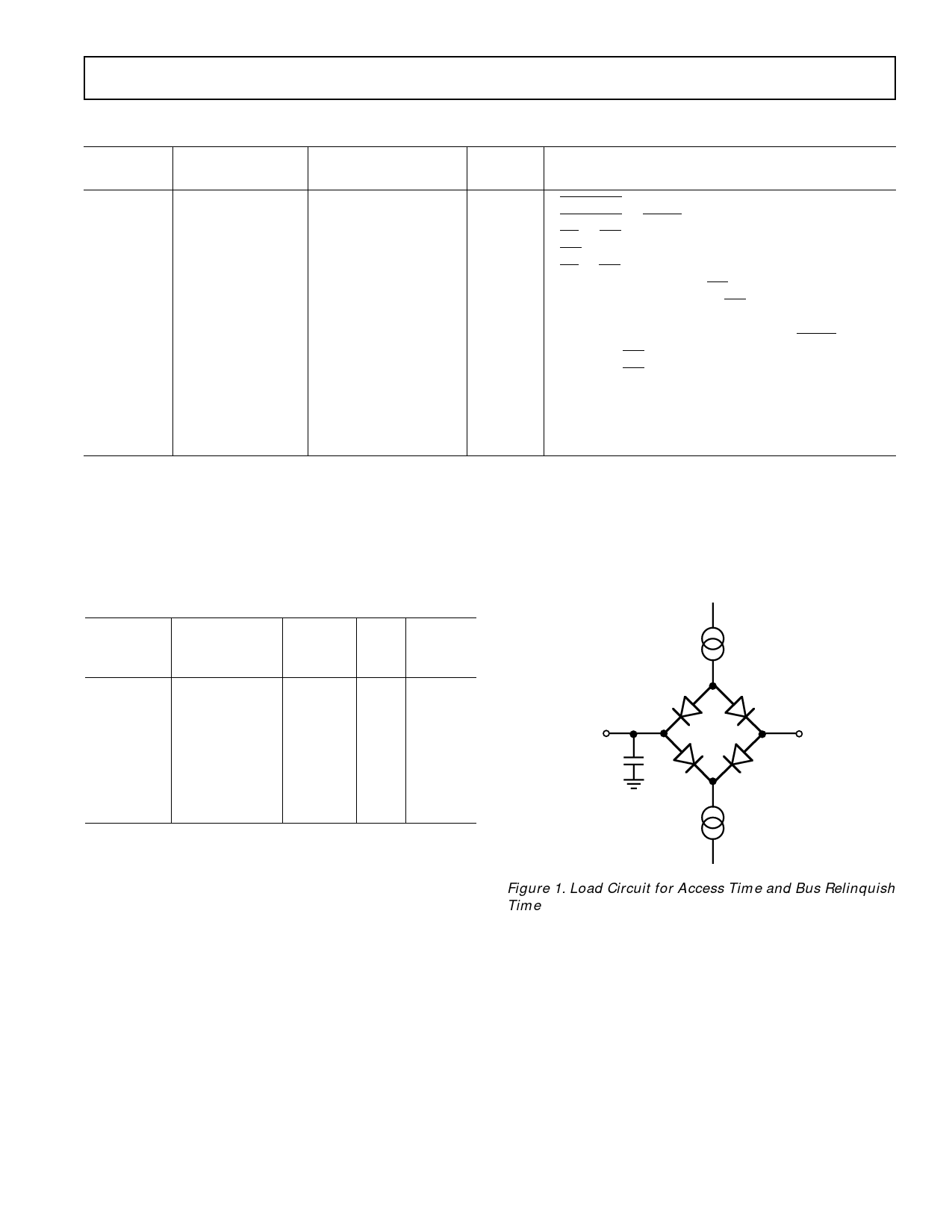
2t6 is measured with the load circuit of Figure 1 and defined as the time required for an output to cross 0.8 V or 2.4 V.
3t7 is derived from the measured time taken by the data outputs to change 0.5 V when loaded with the circuit of Figure 1. The measured number is then extrap-
olated back to remove the effects of charging or discharging the 100 pF capacitor. This means that the time, t 7, quoted in the Timing Characteristics is the true
bus relinquish time of the part and as such is independent of external bus loading capacitances.
Specifications subject to change without notice.
ORDERING GUIDE
Model1
Linearity
Temperature
Range
Error
(% FSR)
SNR
(dB)
Package
Option2
AD7884AN –40°C to +85°C
84
AD7884BN –40°C to +85°C ± 0.0075 84
AD7884AP –40°C to +85°C
84
AD7884BP –40°C to +85°C ± 0.0075 84
AD7885AN –40°C to +85°C
84
AD7885BN –40°C to +85°C ± 0.0075 84
AD7885AAP –40°C to +85°C
84
AD7885ABP –40°C to +85°C ± 0.0075 84
N-40A
N-40A
P-44A
P-44A
N-28A
N-28A
P-44A
P-44A
NOTES
1Analog Devices reserves the right to ship cerdip (Q) packages in lieu of plastic
DIP (N) packages.
2N = Plastic DIP; P = Plastic Leaded Chip Carrier (PLCC).
1.6mA
I OL
TO OUTPUT PIN
CL
100pF
200µA
I OH
+2.1V
Figure 1. Load Circuit for Access Time and Bus Relinquish
Time
REV. C
–3–
Share Link: 