74LVC32ABQ Ver la hoja de datos (PDF) - Philips Electronics
Número de pieza
componentes Descripción
fabricante
74LVC32ABQ Datasheet PDF : 16 Pages
| |||
Philips Semiconductors
Quad 2-input OR gate
Product specification
74LVC32A
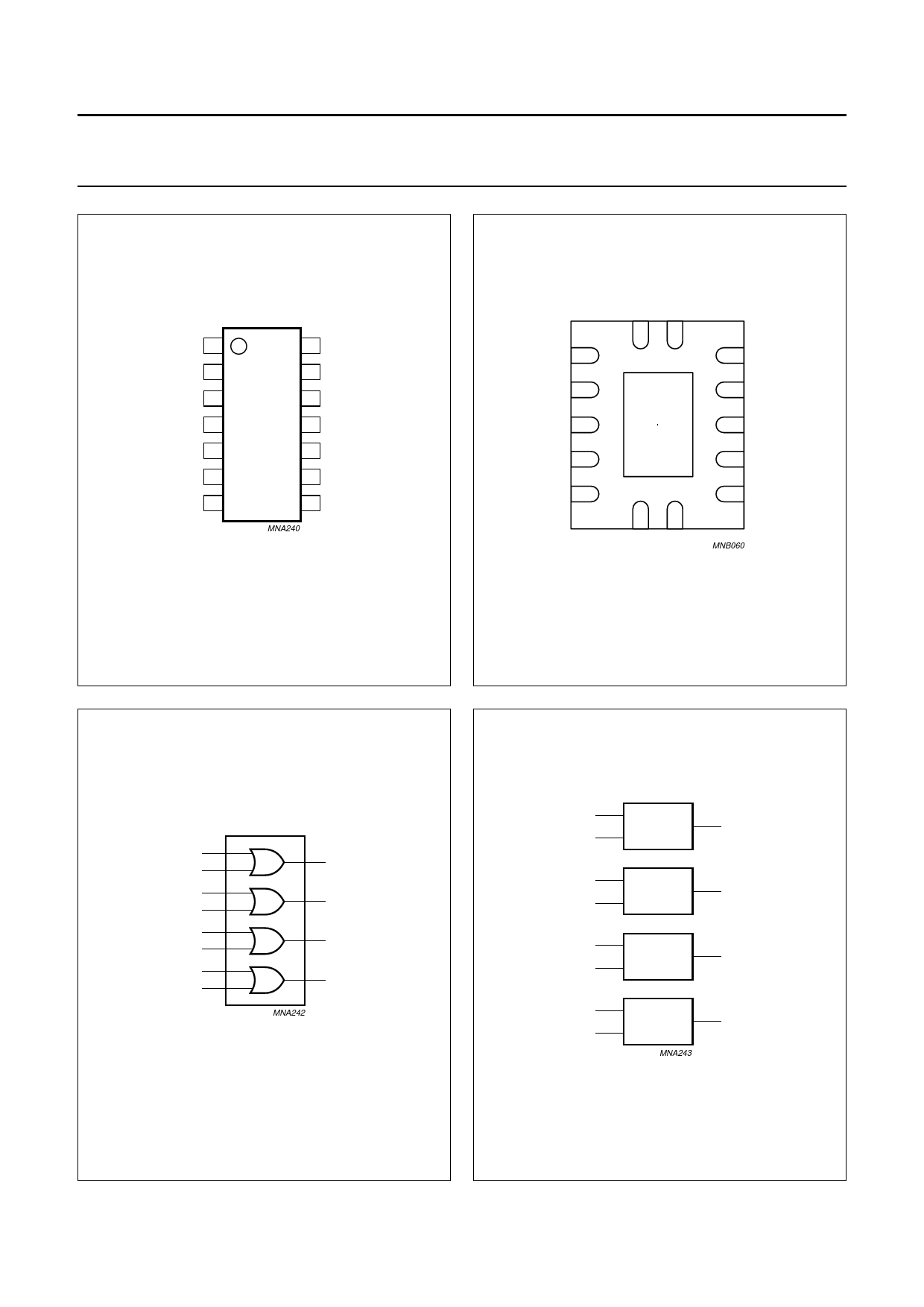
handbook, halfpage
1A 1
1B 2
1Y 3
2A 4
2B 5
2Y 6
GND 7
14 VCC
13 4B
12 4A
32
11 4Y
10 3B
9 3A
8 3Y
MNA240
handbook, halfpage
1B 2
1A VCC
1 14
13 4B
1Y 3
2A 4
GND(1)
12 4A
11 4Y
2B 5
10 3B
2Y 6
78
Top view GND 3Y
9 3A
MNB060
Fig.1 Pin configuration SO14 and (T)SSOP14.
(1) The die substrate is attached to this pad using conductive die
attach material. It can not be used as a supply pin or input.
Fig.2 Pin configuration DHVQFN14.
handbook, halfpage
1 1A
2 1B
4 2A
5 2B
9 3A
10 3B
12 4A
13 4B
1Y 3
2Y 6
3Y 8
4Y 11
MNA242
Fig.3 Logic symbol.
2003 Jul 16
handbook, halfpage
1
2
4
5
9
10
12
13
≥1
3
≥1
6
≥1
8
≥1
11
MNA243
Fig.4 Logic symbol (IEEE/IEC).
4
Share Link: 