74ALVCH16841 Ver la hoja de datos (PDF) - Philips Electronics
Número de pieza
componentes Descripción
fabricante
74ALVCH16841 Datasheet PDF : 10 Pages
| |||
Philips Semiconductors
20-bit bus interface D-type latch (3-State)
Product specification
74ALVCH16841
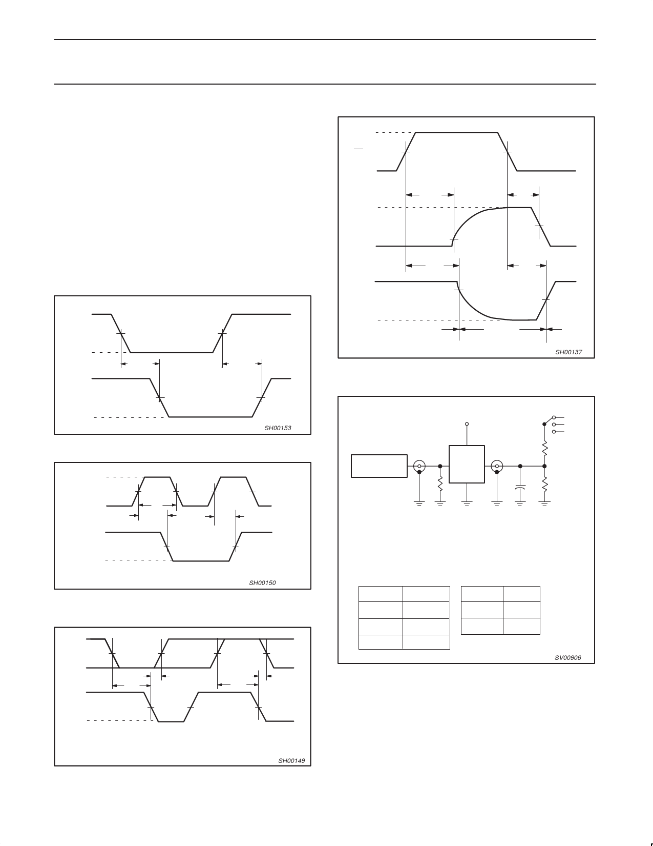
AC WAVEFORMS FOR VCC = 2.3V TO 2.7V AND
VCC < 2.3V RANGE
VM = 0.5 VCC
VX = VOL + 0.15V
VY = VOH –0.15V
VOL and VOH are the typical output voltage drop that occur with the
output load.
AC WAVEFORMS FOR VCC = 3.0V TO 3.6V AND
VCC = 2.7V RANGE
VM = 1.5 V
VX = VOL + 0.3V
VY = VOH –0.3V
VOL and VOH are the typical output voltage drop that occur with the
output load.
VI = 2.7V
VI = VCC
VI
Dn
INPUT
VM
GND
VOH
tPHL
tPLH
Qn
VM
OUTPUT
VOL
SH00153
Waveform 1. The input (Dn) to output (Qn) propagation delay
VI
LE INPUT
GND
VOH
Qn OUTPUT
VOL
VM
tW
tPHL
VM
VM
tPLH
SH00150
Waveform 2. The latch enable (LE) pulse width, the latch enable
input to output (Qn) propagation delay
ÉÉÉ VI
Dn
ÉÉÉ INPUT
VM
ÉÉÉ GND
ÉÉÉÉÉÉÉÉÉÉÉÉÉÉÉÉÉÉÉÉÉÉÉÉÉÉÉ
th
th
tSU
tSU
VI
LE
INPUT
VM
GND
NOTE: The shaded areas indicate when the input is permitted to change
for predictable output performance.
SH00149
Waveform 3. The data set up and hold times for the Dn input to
the LE input
VI
nOE INPUT
VM
GND
VCC
OUTPUT
LOW-to-OFF
OFF-to-LOW
VOL
tPLZ
VX
tPZL
VM
VOH
OUTPUT
HIGH-to-OFF
OFF-to-HIGH
GND
tPHZ
outputs
enabled
tPZH
VY
VM
outputs
disabled
outputs
enabled
SH00137
Waveform 4. 3-State enable and disable times
TEST CIRCUIT
VCC
PULSE
GENERATOR
VI
RT
VO
D.U.T.
CL
S1
2 * VCC
Open
GND
RL = 500 Ω
RL = 500 Ω
Test Circuit for switching times
DEFINITIONS
RL = Load resistor
CL = Load capacitance includes jig and probe capacitance
RT = Termination resistance should be equal to ZOUT of pulse generators.
SWITCH POSITION
TEST
S1
VCC
VI
tPLH/tPHL
Open
< 2.7V
VCC
tPLZ/tPZL
tPHZ/tPZH
2 < VCC
GND
2.7–3.6V
2.7V
SV00906
Waveform 5. Load circuitry for switching times
1998 Jul 27
7
Share Link: 