74ACT245B(1999) Ver la hoja de datos (PDF) - STMicroelectronics
Número de pieza
componentes Descripción
fabricante
74ACT245B Datasheet PDF : 9 Pages
| |||
74ACT245
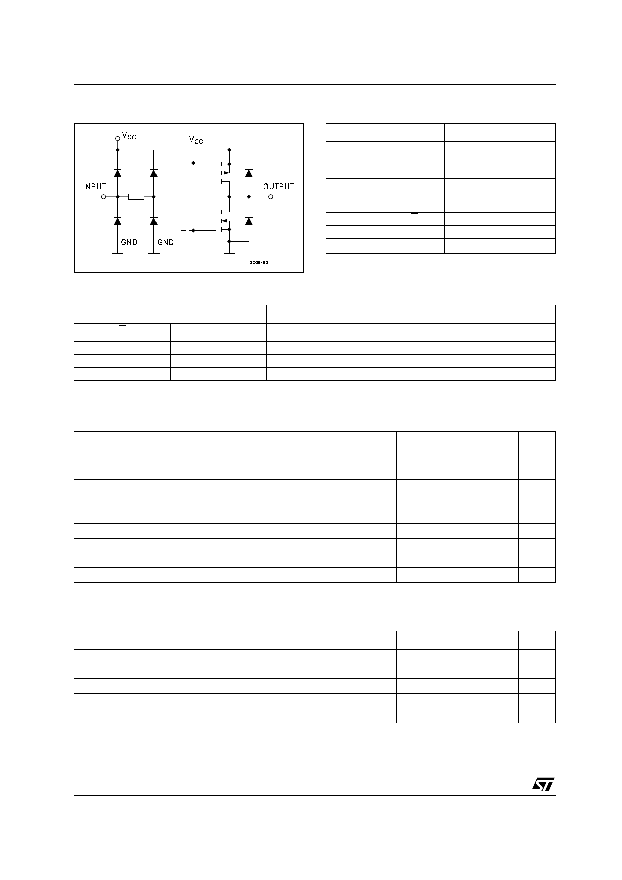
INPUT AND OUTPUT EQUIVALENT CIRCUIT
PIN DESCRIPTION
PIN No
1
2,3, 4,5,
6, 7,8, 9
18, 17, 16,
15, 14, 13,
12, 11
19
10
20
S YM BO L
DIR
A1 to A8
NAME AND FUNCTION
Directional Control
Data Inputs/Outputs
B1 to B8 Data Inputs/Outputs
G
GND
VCC
Output Enabel Input
Ground (0V)
Positive Supply Voltage
TRUTH TABLE
G
L
L
H
X:”H” or ”L”
Z: High impedance
INPUT
DIR
L
H
X
F UN CTI ON
A BUS
B BUS
OUTPUT
INPUT
INPUT
OUTPUT
Z
Z
OUT PUT
A =B
B =A
Z
ABSOLUTE MAXIMUM RATINGS
Symbol
Parameter
Value
Unit
VCC Supply Voltage
-0.5 to +7
V
VI
DC Input Voltage
-0.5 to VCC + 0.5
V
VO DC Output Voltage
-0.5 to VCC + 0.5
V
IIK
DC Input Diode Current
± 20
mA
IOK DC Output Diode Current
± 20
mA
IO
DC Output Current
± 50
mA
ICC orIGND DC VCC or Ground Current
± 400
mA
Tstg Storage Temperature
-65 to +150
oC
TL
Lead Temperature (10 sec)
300
oC
Absolute Maximum Ratings are those values beyond which damage to the device may occur. Functional operation under these condition is not implied.
RECOMMENDED OPERATING CONDITIONS
Symbol
Pa ram et er
VCC Supply Voltage
VI
Input Voltage
VO
Output Voltage
Top Operating Temperature:
dt/dv Input Rise and Fall Time VCC = 4.5 to 5.5V (note 1)
1) VIN from 0.8 V to 2.0 V
Value
4.5 to 5.5
0 to VCC
0 to VCC
-40 to +85
8
Unit
V
V
V
oC
ns/V
2/9
Share Link: 