2SA673AKCTZ-E Ver la hoja de datos (PDF) - Renesas Electronics
Número de pieza
componentes Descripción
fabricante
2SA673AKCTZ-E Datasheet PDF : 6 Pages
| |||
2SA673A(K)
Preliminary
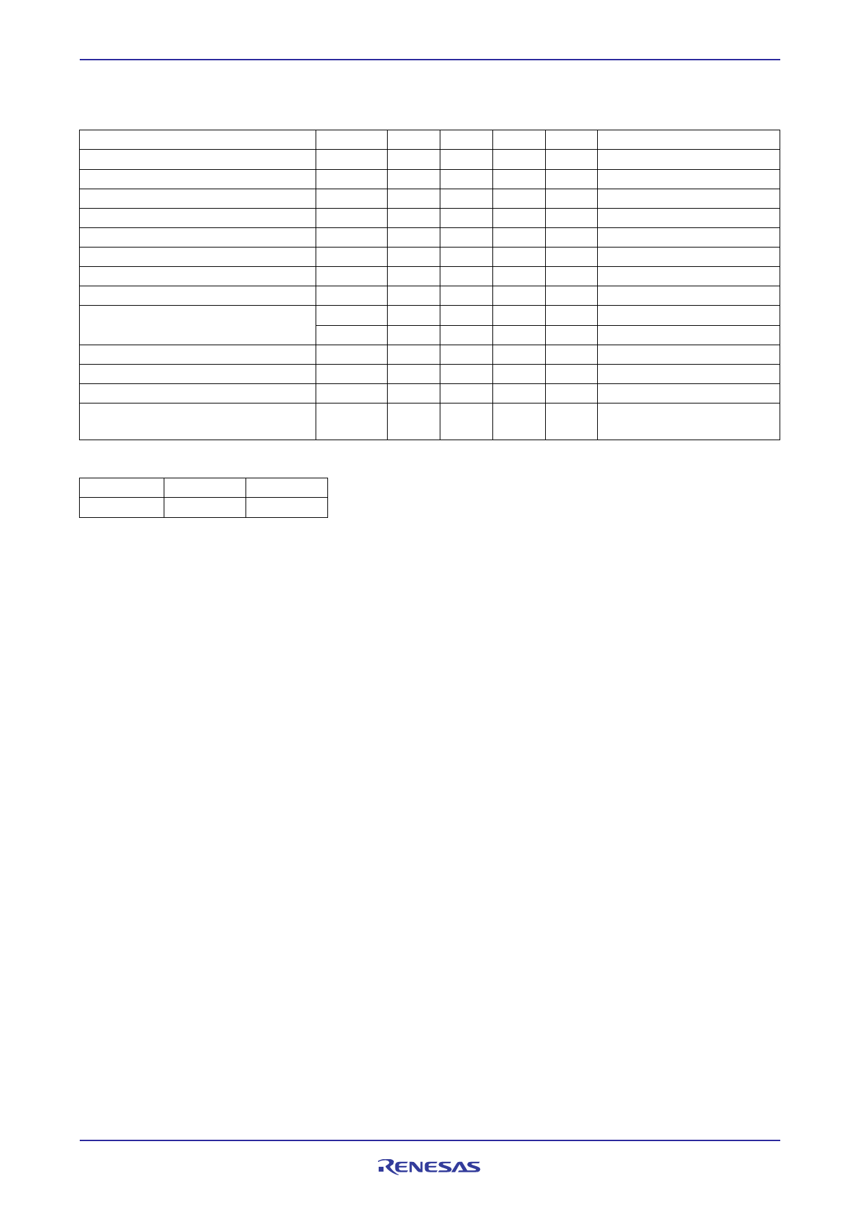
Electrical Characteristics
Item
Symbol Min
Collector to base breakdown voltage
V(BR)CBO
–50
Collector to emitter breakdown voltage V(BR)CEO –50
Emitter to base breakdown voltage
V(BR)EBO
–4
Collector cutoff current
ICBO
—
Emitter cutoff current
IEBO
—
Base to emitter voltage
VBE
—
Collector to emitter saturation voltage
VCE(sat)
—
Base to emitter saturation voltage
DC current transfer ratio
VBE(sat)
—
hFE*1
60
hFE
10
Gain bandwidth product
fT
—
Turn on time
ton
—
Turn off time
toff
—
Storage time
tstg
—
Notes: 1. The 2SA673A(K) is grouped by hFE as follows.
2. Pulse test
B
C
D
60 to 120 100 to 200 160 to 320
Typ Max
—
—
—
—
—
—
—
–0.5
—
–0.5
–0.64 —
–0.2 –0.6
–0.87 —
—
320
—
—
120
—
0.3
—
0.6
—
0.4
—
Unit
V
V
V
μA
μA
V
V
V
MHz
μs
μs
μs
(Ta = 25°C)
Test conditions
IC = –10 µA, IE = 0
IC = –1 mA, RBE = ∞
IE = –10 μA, IC = 0
VCE = –20 V, IE = 0
VEB = –3 V, IC = 0
VCE = –3 V, IC = –10 mA
IC = –150 mA, IB = –15 mA*2
IC = –150 mA, IB = –15 mA*2
VCE = –3 V, IC = –10 mA
VCE = –3 V, IC = –500 mA*2
VCE = –3 V, IC = –10 mA
VCC = –10.3 V
IC = 10 IB1 = –10 IB2 = –10 mA
VCC = –5 V,
IC = IB1 = IB2 = –20 mA
R07DS0430EJ0400 Rev.4.00
Jun 07, 2011
Page 2 of 5
Share Link: 