24C01CT-IMS Ver la hoja de datos (PDF) - Microchip Technology
Número de pieza
componentes Descripción
fabricante
24C01CT-IMS Datasheet PDF : 30 Pages
| |||
24C01C
1.0 ELECTRICAL CHARACTERISTICS
Absolute Maximum Ratings(†)
VCC.............................................................................................................................................................................7.0V
All inputs and outputs w.r.t. VSS ......................................................................................................... -0.6V to VCC +1.0V
Storage temperature ...............................................................................................................................-65°C to +150°C
Ambient temperature with power applied ................................................................................................-40°C to +125°C
ESD protection on all pins ......................................................................................................................................................≥ 4 kV
† NOTICE: Stresses above those listed under “Absolute Maximum Ratings” may cause permanent damage to the
device. This is a stress rating only and functional operation of the device at these or any other conditions above those
indicated in the operational listings of this specification is not implied. Exposure to Absolute Maximum Rating
conditions for extended periods may affect device reliability.
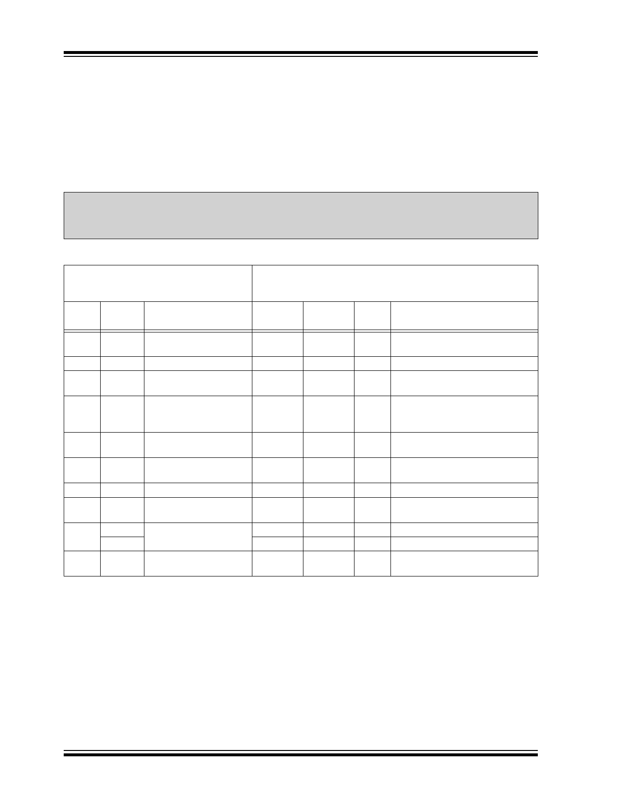
TABLE 1-1: DC CHARACTERISTICS
DC CHARACTERISTICS
Electrical Characteristics:
Industrial (I): VCC = +4.5V to 5.5V
Automotive (E): VCC = +4.5V to 5.5V
Param.
No.
Sym.
Characteristic
Min.
Max. Units
D1
—
D2
VIH
D3
VIL
A0, A1, A2, SCL, SDA
and WP pins:
High-level input voltage
Low-level input voltage
—
0.7 VCC
—
—
—
0.3 VCC
——
V—
V—
TA = -40°C to +85°C
TA = -40°C to +125°C
Conditions
D4
VHYS Hysteresis of Schmitt
0.05 VCC
—
Trigger inputs
(SDA, SCL pins)
D5
VOL
Low-level output voltage
—
0.40
V (Note)
V IOL = 3.0 mA @ VCC = 4.5V
D6
ILI
Input leakage current
—
±1
μA VIN = VSS or VCC, WP = VSS
D7
ILO
Output leakage current
—
D8
CIN,
Pin capacitance
—
COUT (all inputs/outputs)
D9
ICC Read Operating current
—
ICC Write
—
D10 ICCS
Standby current
—
±1
μA
10
pF
1
mA
3
mA
5
μA
Note: This parameter is periodically sampled and not 100% tested.
VOUT = VSS or VCC
VCC = 5.0V (Note)
TA = 25°C, f = 1 MHz
VCC = 5.5V, SCL = 400 kHz
VCC = 5.5V
VCC = 5.5V, SDA = SCL = VCC
WP = VSS
DS21201J-page 2
© 2008 Microchip Technology Inc.
Share Link: 