AD569JP Ver la hoja de datos (PDF) - Analog Devices
Número de pieza
componentes Descripción
fabricante
AD569JP Datasheet PDF : 12 Pages
| |||
AD569
AC PERFORMANCE CHARACTERISTICS
These characteristics are included for Design Guidance Only and are not subject to test.
+VS = +12 V; –VS = –12 V; +VREF = +5 V; –VREF = –5 V excepts where stated.
Parameter
Limit
Units
Test Conditions/Comments
Output Voltage Settling
5
(Time to ± 0.001% FS
3
For FS Step)
6
4
µs max
µs typ
µs max
µs typ
No Load Applied
(DAC output measured from falling edge of LDAC.)
VOUT Load = 1 kΩ, CLOAD = 1000 pF.
(DAC output measured from falling edge of LDAC. )
Digital-to-Analog Glitch
500
Impulse
nV-sec typ
Measured with VREF = 0 V. DAC registers alternatively loaded
with input codes of 8000H and 0FFFH (worst-case
transition). Load = 1 kΩ.
Multiplying Feedthrough
Output Noise Voltage
Density (1 kHz-1 MHz)
–100
40
dB max
nV/͙Hz typ
+VREF = 1 V rms 10 kHz sine wave,
–VREF = 0 V
Measured between VOUT and –VREF
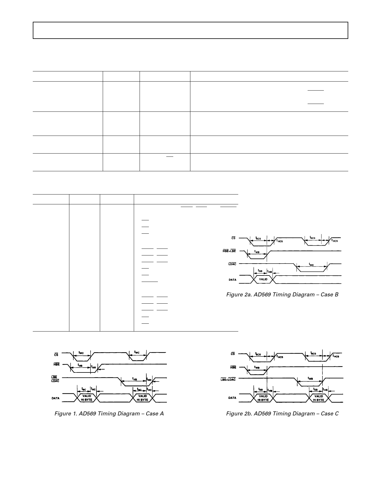
TIMING CHARACTERISTICS (+VS = +12 V, –VS = –12 V, VIH = 2.4 V, VIL = 0.4 V,TMIN to TMAX)
Parameter
Case A
tWC
tSC
tHC
Case B
tWB
tSB
tHB
tSCS
tHCS
tWD
Case C
tWB
tSB
tHB
tSCS
tHCS
Limit
120
60
20
70
80
20
120
10
120
120
80
20
120
10
Units
ns min
ns min
ns min
ns min
ns min
ns min
ns min
ns min
ns min
ns min
ns min
ns min
ns min
ns min
Test Conditions/Comments
150 ns Pulse on HBE, LBE, and LDAC
THS = 140 ns min, THH = 10 ns min
CS Pulse Width
CS Data Setup Time
CS Data Hold Time
None
HBE, LBE Pulse Width
HBE, LBE Data Setup Time
HBE, LBE Data Hold Time
CS Setup Time
CS Hold Time
LDAC Pulse Width
None
HBE, LBE Pulse Width
HBE, LBE Data Setup Time
Figure 2a. AD569 Timing Diagram – Case B
HBE, LBE Data Hold Time
CS Setup Time
CS Hold Time
Figure 1. AD569 Timing Diagram – Case A
Figure 2b. AD569 Timing Diagram – Case C
REV. A
–3–
Share Link: 