IXFN230N20T Ver la hoja de datos (PDF) - IXYS CORPORATION
Número de pieza
componentes Descripción
fabricante
IXFN230N20T Datasheet PDF : 5 Pages
| |||
IXFN230N20T
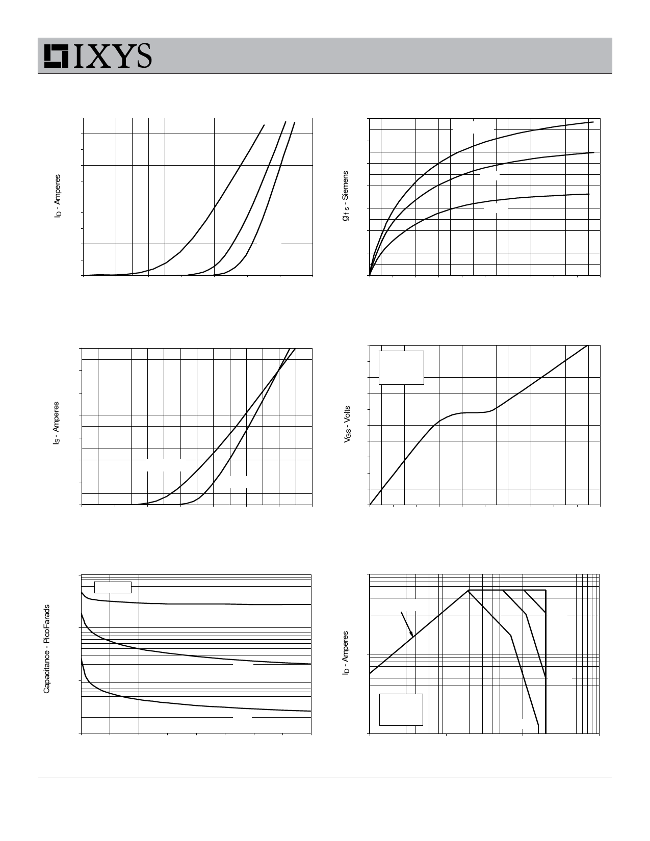
Fig. 7. Input Admittance
200
180
160
140
120
100
TJ = 150ºC
80
25ºC
60
40
- 40ºC
20
0
3.0
3.5
4.0
4.5
5.0
5.5
6.0
6.5
VGS - Volts
Fig. 9. Forward Voltage Drop of
Intrinsic Diode
350
300
250
200
150
100
TJ = 150ºC
50
TJ = 25ºC
0
0.0
0.2
0.4
0.6
0.8
1.0
1.2
1.4
VSD - Volts
Fig. 8. Transconductance
280
TJ = - 40ºC
240
200
25ºC
160
120
150ºC
80
40
0
0 20 40 60 80 100 120 140 160 180 200
ID - Amperes
Fig. 10. Gate Charge
10
9
VDS = 100V
I D = 115A
8
I G = 10mA
7
6
5
4
3
2
1
0
0 40 80 120 160 200 240 280 320 360 400
QG - NanoCoulombs
100,000
Fig. 11. Capacitance
f = 1 MHz
10,000
Ciss
1,000
Fig. 12. Forward-Bias Safe Operating Area
RDS(on) Limit
25µs
1,000
Coss
100
0
Crss
5
10
15
20
25
30
35
40
VDS - Volts
IXYS Reserves the Right to Change Limits, Test Conditions, and Dimensions.
100
10
1
TJ = 175ºC
TC = 25ºC
Single Pulse
10
VDS - Volts
100µs
1ms
100
1000
IXYS REF: F_230N20T (9E)03-25-09
Share Link: 