AD7871TQ Ver la hoja de datos (PDF) - Analog Devices
Número de pieza
componentes Descripción
fabricante
AD7871TQ Datasheet PDF : 16 Pages
| |||
AD7871/AD7872
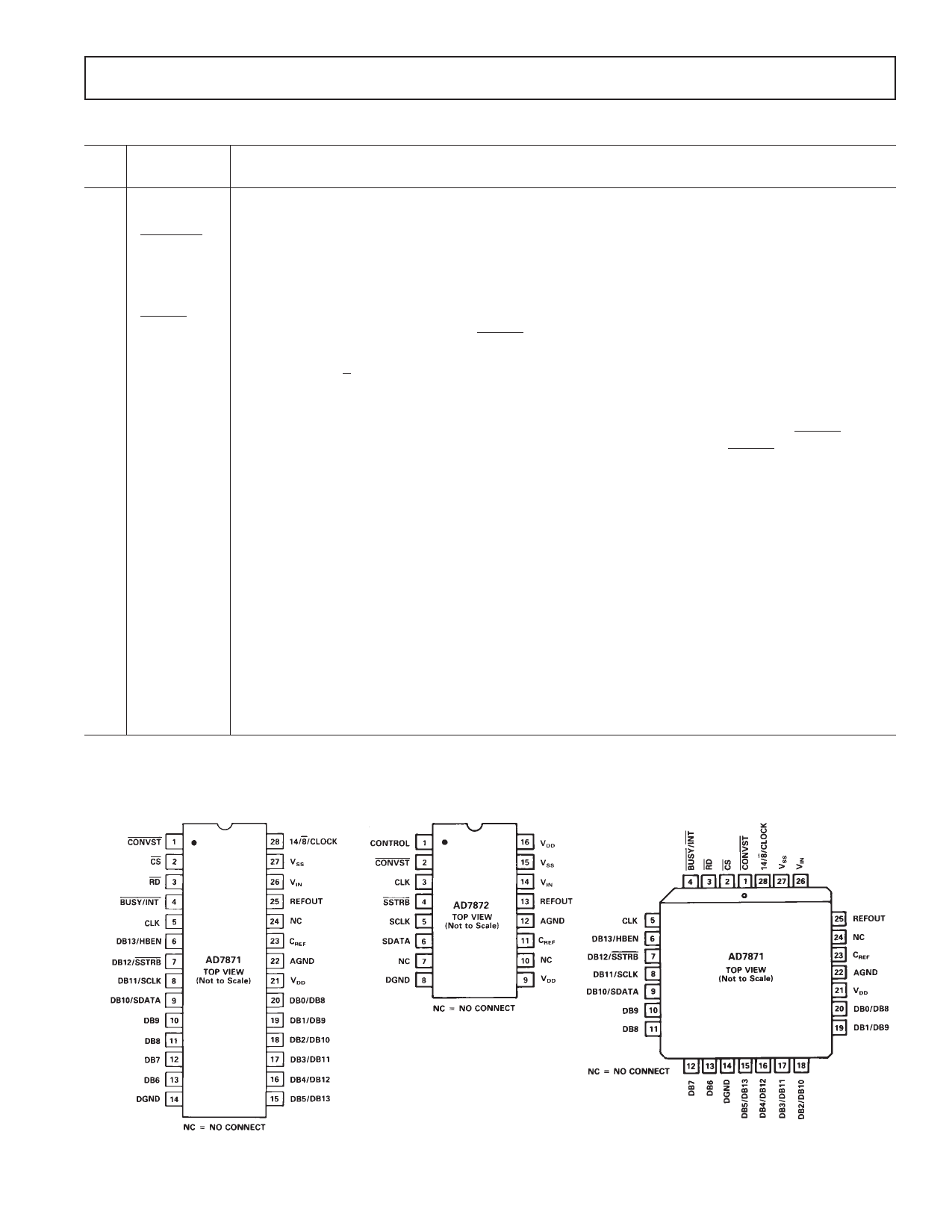
AD7872 PIN FUNCTION DESCRIPTION
DIP
No. Mnemonic
1
CONTROL
2
CONVST
3
CLK
4
SSTRB
5
SCLK
6
SDATA
7
NC
8
DGND
9
VDD
10
NC
11
CREF
12
AGND
13
REF OUT
14
VIN
15
VSS
16
VDD
Function
Control Input. With this pin at 0 V, the SCLK is noncontinuous; with this pin at –5 V, the SCLK
is continuous.
Convert Start. A low to high transition on this input puts the track/hold into the hold mode. This
input is asynchronous to the CLK.
Clock Input. An external TTL-compatible clock may be applied to this input. Alternatively, tying
this pin to VSS, enables the internal laser-trimmed oscillator.
This is an active low three-state output that provides a framing pulse for serial data. An external
4.7 kΩ pull-up resistor is required on SSTRB.
Serial Clock. SCLK is the gated serial clock output derived from the internal or external ADC
clock. If the 14/8/CLK input is at –5 V, then the SCLK runs continuously. With CONTROL
at 0 V, it is gated off (three-state) after serial transmission is complete. SCLK is an open-drain
output and requires an external 2 kΩ pull-up resistor.
Serial Data. This is the three-state serial data output used in conjunction with SCLK and SSTRB in
serial data transmission. Serial data is valid on the falling edge of SCLK, when SSTRB is low. An
external 4.7 kΩ pull-up resistor is required on SDATA.
No Connect.
Digital Ground. Ground return for digital circuitry.
Positive Supply for analog circuitry, +5 V ± 5%.
No Connect.
Decoupling point for on-chip reference. Connect 10 nF capacitor between this pin and AGND.
Analog Ground. Ground reference for analog circuitry.
Voltage Reference Output. The internal 3 V reference is provided at this pin. The external load
capability is 500 µA.
Analog Input. The input range is ± 3 V.
Negative Supply, –5 V ± 5%.
Positive Supply for analog circuitry, +5 V ± 5%. Pin 16 and Pin 9 should be connected together.
PIN CONFIGURATIONS
DIP
DIP, SOIC
PLCC
REV. D
–5–
Share Link: 