P8NK80Z(2003) View Datasheet(PDF) - STMicroelectronics
Part Name
Description
MFG CO.
P8NK80Z
(Rev.:2003)
(Rev.:2003)
STMicroelectronics
P8NK80Z Datasheet PDF : 11 Pages
| |||
STP8NK80Z - STP8NK80ZFP - STW8NK80Z
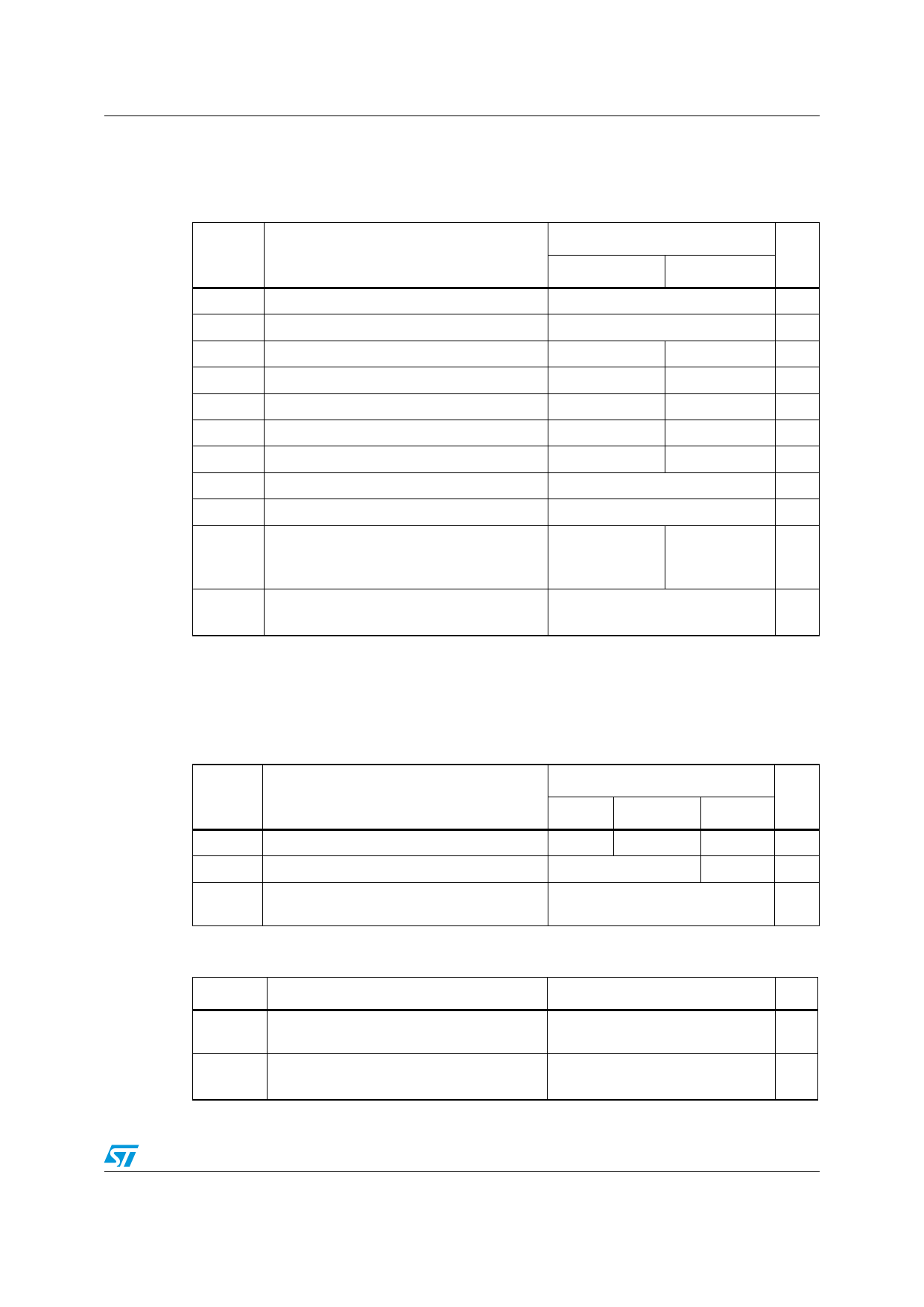
ELECTRICAL CHARACTERISTICS (TCASE =25°C UNLESS OTHERWISE SPECIFIED)
ON/OFF
Symbol
Parameter
Test Conditions
Min. Typ. Max. Unit
V(BR)DSS Drain-source
ID = 1 mA, VGS = 0
800
V
Breakdown Voltage
IDSS
Zero Gate Voltage
Drain Current (VGS = 0)
VDS = Max Rating
VDS = Max Rating, TC = 125 °C
1
µA
50
µA
IGSS
Gate-body Leakage
Current (VDS = 0)
VGS = ± 20V
±10
µA
VGS(th) Gate Threshold Voltage
VDS = VGS, ID = 100 µA
3
3.75
4.5
V
RDS(on)
Static Drain-source On
Resistance
VGS = 10 V, ID = 3.1 A
1.3
1.5
Ω
DYNAMIC
Symbol
Parameter
gfs (1) Forward Transconductance
Ciss
Coss
Crss
Input Capacitance
Output Capacitance
Reverse Transfer
Capacitance
Coss eq. (3) Equivalent Output
Capacitance
SWITCHING ON
Symbol
Parameter
td(on)
tr
Turn-on Delay Time
Rise Time
Qg
Total Gate Charge
Qgs
Gate-Source Charge
Qgd
Gate-Drain Charge
Test Conditions
VDS = 15 V, ID = 3.1 A
VDS = 25 V, f = 1 MHz, VGS = 0
Min.
VGS = 0, VDS = 640 V
Test Conditions
VDD = 400 V, ID = 3.1 A
RG = 4.7Ω, VGS = 10 V
(Resistive Load see, Figure 3)
VDD = 640 V, ID = 6.2 A,
VGS = 10 V
Min.
Typ.
5.2
1320
143
27
58
Typ.
17
30
46
8.5
25
Max. Unit
S
pF
pF
pF
pF
Max. Unit
ns
ns
nC
nC
nC
SWITCHING OFF
Symbol
Parameter
td(off)
tf
Turn-off Delay Time
Fall Time
tr(Voff)
tf
tc
Off-voltage Rise Time
Fall Time
Cross-over Time
Test Conditions
VDD = 400 V, ID = 3.1 A
RG = 4.7Ω VGS = 10 V
(Resistive Load see, Figure 3)
VDD = 640V, ID = 6.2 A,
RG = 4.7Ω, VGS = 10 V
(Inductive Load see, Figure 5)
Min.
Typ.
48
28
9
9
18
Max. Unit
ns
ns
ns
ns
ns
SOURCE DRAIN DIODE
Symbol
Parameter
Test Conditions
Min. Typ. Max. Unit
ISD
ISDM (2)
Source-drain Current
Source-drain Current (pulsed)
6.2
A
24.8
A
VSD (1) Forward On Voltage
ISD = 6.2 A, VGS = 0
1.6
V
trr
Qrr
IRRM
Reverse Recovery Time
Reverse Recovery Charge
Reverse Recovery Current
ISD = 6.2 A, di/dt = 100 A/µs
VDD = 50 V, Tj = 150°C
(see test circuit, Figure 5)
460
ns
2990
nC
13
A
Note: 1. Pulsed: Pulse duration = 300 µs, duty cycle 1.5 %.
2. Pulse width limited by safe operating area.
3. Coss eq. is defined as a constant equivalent capacitance giving the same charging time as Coss when VDS increases from 0 to 80%
VDSS.
3/11
Share Link: 