STD5NM60-1(2003) View Datasheet(PDF) - STMicroelectronics
Part Name
Description
MFG CO.
STD5NM60-1
(Rev.:2003)
(Rev.:2003)
STMicroelectronics
STD5NM60-1 Datasheet PDF : 13 Pages
| |||
STP8NM60, STP8NM60FP, STD5NM60, STD5NM60-1
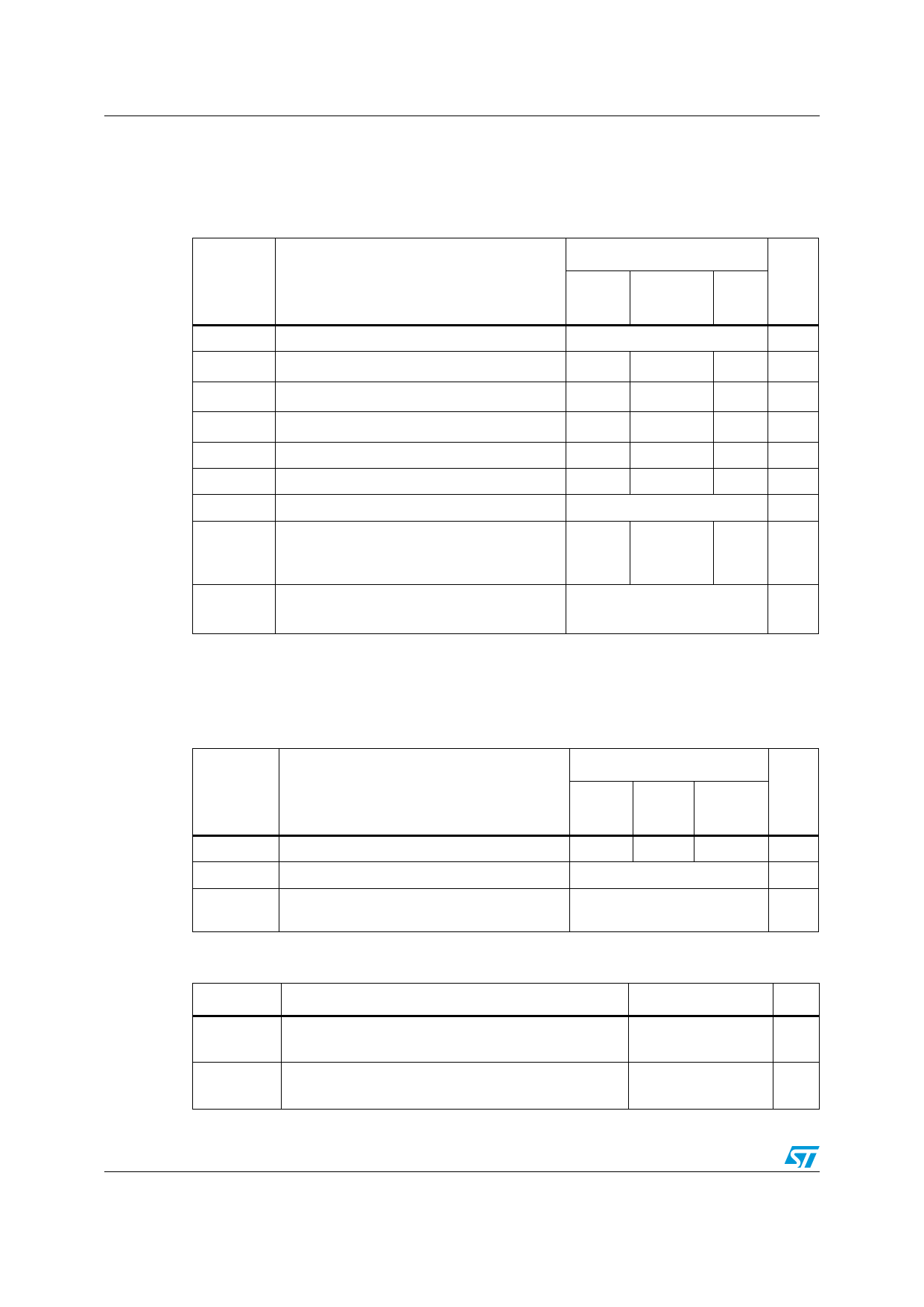
ABSOLUTE MAXIMUM RATINGS
Symbol
Parameter
VDS
Drain-source Voltage (VGS = 0)
VDGR
Drain-gate Voltage (RGS = 20 kΩ)
VGS
Gate- source Voltage
ID
Drain Current (continuous) at TC = 25°C
ID
Drain Current (continuous) at TC = 100°C
IDM ( ) Drain Current (pulsed)
PTOT
Total Dissipation at TC = 25°C
Derating Factor
dv/dt (1) Peak Diode Recovery voltage slope
VISO
Insulation Withstand Voltage (DC)
Tj
Operating Junction Temperature
Tstg
Storage Temperature
( ) Pulse width limited by safe operating area
(1) ISD ≤5A, di/dt ≤400A/µs, VDD ≤ V(BR)DSS, Tj ≤ TJMAX.
(*) Limited only by maximum temperature allowed
STP8NM60
8
5
32
100
0.8
15
-
Value
STP8NM60FP
600
600
± 30
8 (*)
5 (*)
32 (*)
30
0.24
15
2500
-55 to 150
-55 to 150
STD5NM60
STD5NM60-1
5
3.1
20
96
0.4
15
-
THERMAL DATA
Rthj-case
Rthj-amb
Tl
Thermal Resistance Junction-case Max
Thermal Resistance Junction-ambient Max
Maximum Lead Temperature For Soldering Purpose
TO-220
1.25
TO-220FP
4.16
62.5
300
DPAK
IPAK
1.3
Unit
V
V
V
A
A
A
W
W/°C
V/ns
V
°C
°C
°C/W
°C/W
°C
AVALANCHE CHARACTERISTICS
Symbol
Parameter
IAR
Avalanche Current, Repetitive or Not-Repetitive
(pulse width limited by Tj max)
EAS
Single Pulse Avalanche Energy
(starting Tj = 25 °C, ID = IAR, VDD = 50 V)
Max Value
Unit
2.5
A
200
mJ
ELECTRICAL CHARACTERISTICS (TCASE =25°C UNLESS OTHERWISE SPECIFIED)
ON/OFF
Symbol
Parameter
Test Conditions
Min. Typ. Max.
V(BR)DSS Drain-source
ID = 250 µA, VGS = 0
600
Breakdown Voltage
IDSS
Zero Gate Voltage
VDS = Max Rating
1
Drain Current (VGS = 0)
VDS = Max Rating, TC = 125 °C
10
IGSS
Gate-body Leakage
Current (VDS = 0)
VGS = ± 30V
±100
VGS(th) Gate Threshold Voltage
VDS = VGS, ID = 250µA
3
4
5
RDS(on)
Static Drain-source On
Resistance
VGS = 10V, ID = 2.5 A
0.9
1
Unit
V
µA
µA
nA
V
Ω
2/13
Share Link: 