STGB3NB60SD View Datasheet(PDF) - STMicroelectronics
Part Name
Description
MFG CO.
STGB3NB60SD Datasheet PDF : 8 Pages
| |||
STGB3NB60SD
ELECTRICAL CHARACTERISTICS (continued)
SWITCHING OFF
Symbol
Parameter
Test Conditions
tc
tr(Voff)
td(Voff)
tf
Eoff(**)
Cross-Over Time
Off Voltage Rise Time
Delay Time
Fall Time
Turn-off Switching Loss
VCC = 480 V
RGE = 1 kΩ
IC = 3 A
VGE = 15 V
tc
tr(Voff)
td(Voff)
tf
Eoff(**)
Cross-Over Time
Off Voltage Rise Time
Delay Time
Fall Time
Turn-off Switching Loss
VCC = 480 V
RGE = 1 kΩ
Tj = 125 °C
IC = 3 A
VGE = 15 V
Min.
Typ.
1.8
1.0
3.4
0.72
1.15
2.8
1.45
3.6
1.2
1.8
Max.
Unit
µs
µs
µs
µs
mJ
µs
µs
µs
µs
mJ
COLLECTOR-EMITTER DIODE
Symbol
Parameter
Test Conditions
If
Forward Current
Ifm
Forward Current pulsed
Vf
Forward On-Voltage
If = 3 A
If = 1 A
trr
Reverse Recovery Time
If = 3 A
Qrr
Reverse Recovery Charge di/dt = 100 A/µs
Irrm
Reverse Recovery Current
(•)Pulse width limited by max. junction temperature
(*)Pulsed: Pulse duration = 300 µs, duty cycle 1.5 %.
(∗∗)Losses Include Also The Tail (Jedec Standardization)
VR = 200 V
Tj = 125 °C
Min.
Typ.
1.55
1.15
1700
4500
9.5
Max.
3
25
1.9
Unit
A
A
V
V
ns
nC
A
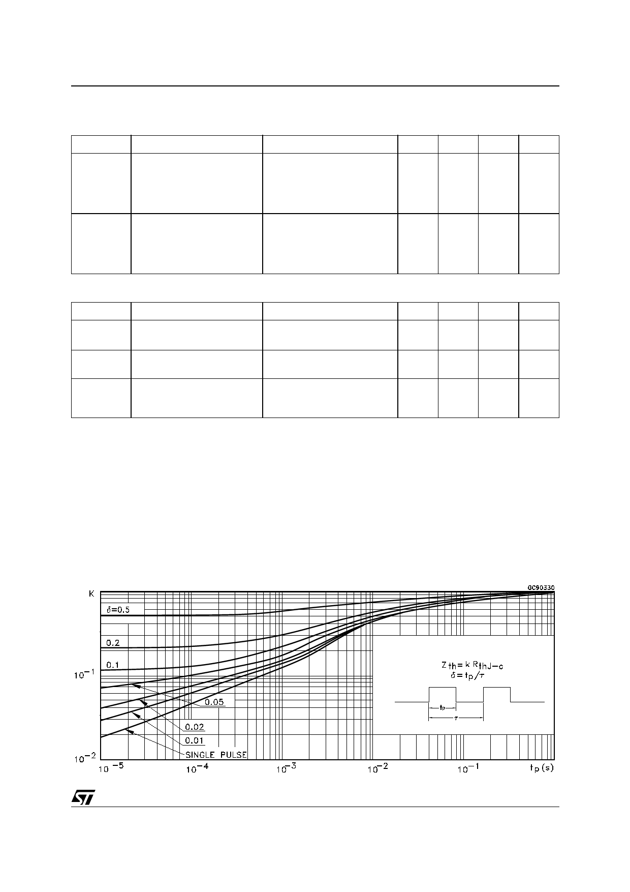
Thermal Impedance
3/8
Share Link: 