STB10NB20T4 View Datasheet(PDF) - STMicroelectronics
Part Name
Description
MFG CO.
STB10NB20T4 Datasheet PDF : 8 Pages
| |||
STB10NB20
ELECTRICAL CHARACTERISTICS (continued)
SWITCHING ON
Symbol
Parameter
Test Conditions
Min. Typ. Max. Unit
td(on)
tr
Turn-on Delay Time Rise Time VDD = 100 V
RG = 4.7 Ω
ID = 5 A
VGS = 10 V
(see test circuit, Figure 3)
10
14
ns
15
20
ns
Qg
Total Gate Charge
Qgs
Gate-Source Charge
Qgd
Gate-Drain Charge
VDD=160V ID=10A VGS=10V
17
24
nC
7.5
nC
5.5
nC
SWITCHING OFF
Symbol
Parameter
tr(Voff)
tr
tc
Off-voltage Rise Time
Fall Time
Cross-over Time
Test Conditions
VDD = 160 V
RG = 4.7 Ω
ID = 10 A
VGS = 10 V
(see test circuit, Figure 5)
Min.
Typ.
8
10
20
Max.
11
14
28
Unit
ns
ns
ns
SOURCE DRAIN DIODE
Symbol
Parameter
Test Conditions
ISD
ISDM (•)
Source-drain Current
Source-drain Current (pulsed)
VSD (*) Forward On Voltage
ISD = 10 A
VGS = 0
trr
Qrr
IRRM
Reverse Recovery Time
Reverse Recovery Charge
Reverse Recovery Current
ISD = 10 A di/dt = 100 A/µs
VDD = 50 V
Tj = 150 °C
(see test circuit, Figure 5)
(*)Pulsed: Pulse duration = 300 µs, duty cycle 1.5 %.
(•)Pulse width limit ed by safe operating area.
Min.
Typ.
170
980
11.5
Max.
10
40
1.5
Unit
A
A
V
ns
nC
A
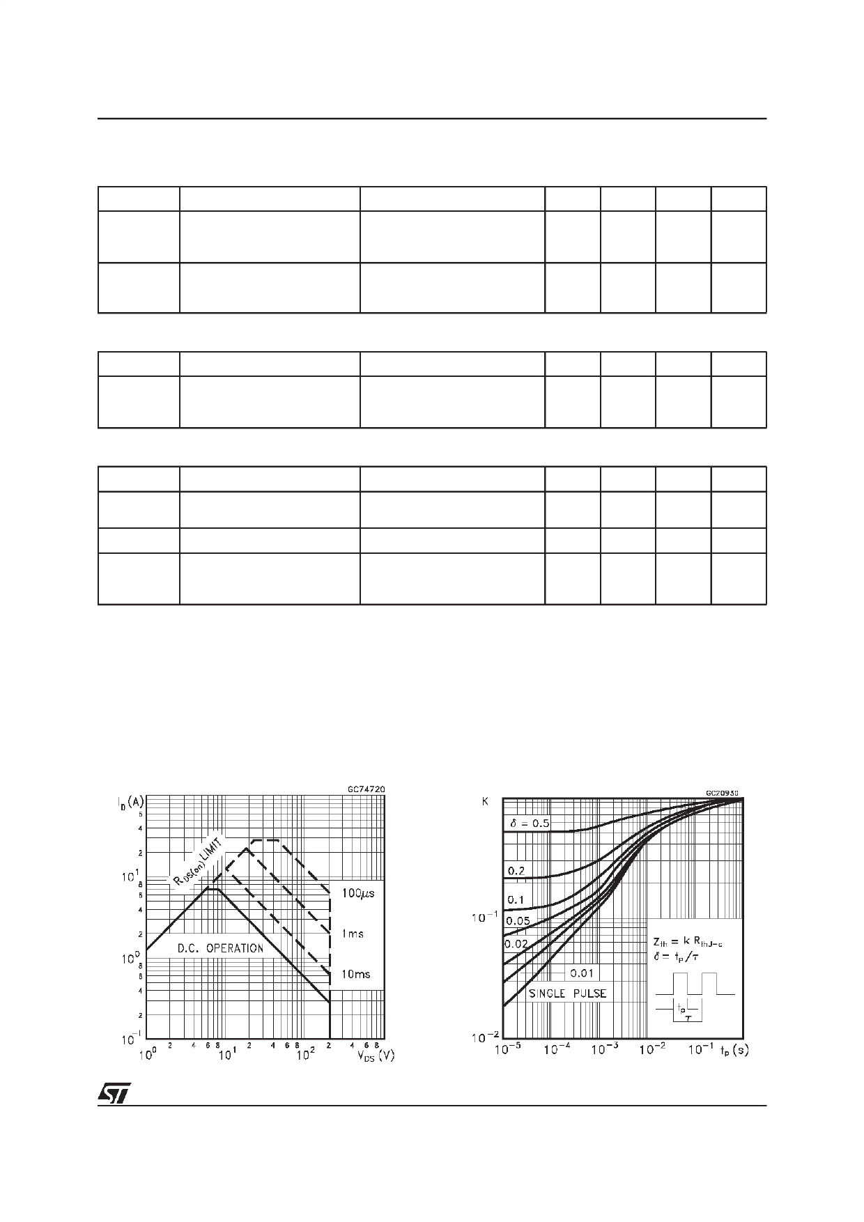
Safe Operating Area
Thermal Impedance
3/8
Share Link: 