LTC2942C(RevA) View Datasheet(PDF) - Linear Technology
Part Name
Description
MFG CO.
LTC2942C Datasheet PDF : 18 Pages
| |||
LTC2942
Pin Functions
SENSE+ (Pin 1): Positive Current Sense Input and Power
Supply. Connect to the load/charger side of the sense
resistor. VSENSE+ operating range is 2.7V to 5.5V.
GND (Pin 2): Device Ground. Connect directly to the nega-
tive battery terminal.
SCL (Pin 3): Serial Bus Clock Input.
SDA (Pin 4): Serial Bus Data Input and Output.
AL/CC (Pin 5): Alert Output or Charge Complete Input.
Configured either as an SMBus alert output or charge
complete input by control register bits B[2:1]. At power-up,
the pin defaults to alert mode conforming to the SMBus
alert response protocol. It behaves as an open-drain logic
output that pulls to GND when any threshold register value
is exceeded. When configured as a charge complete input,
connect to the charge complete output from the battery
charger circuit. A high level at CC sets the value of the
accumulated charge (registers C, D) to FFFFh.
SENSE– (Pin 6): Negative Current Sense Input. Connect
SENSE– to the positive battery terminal side of the sense
resistor. The voltage between SENSE– and SENSE+ must
remain within ±50mV in normal operation. SENSE– is also
the input for the ADC in voltage measurement mode.
Exposed Pad (Pin 7): Do Not Connect.
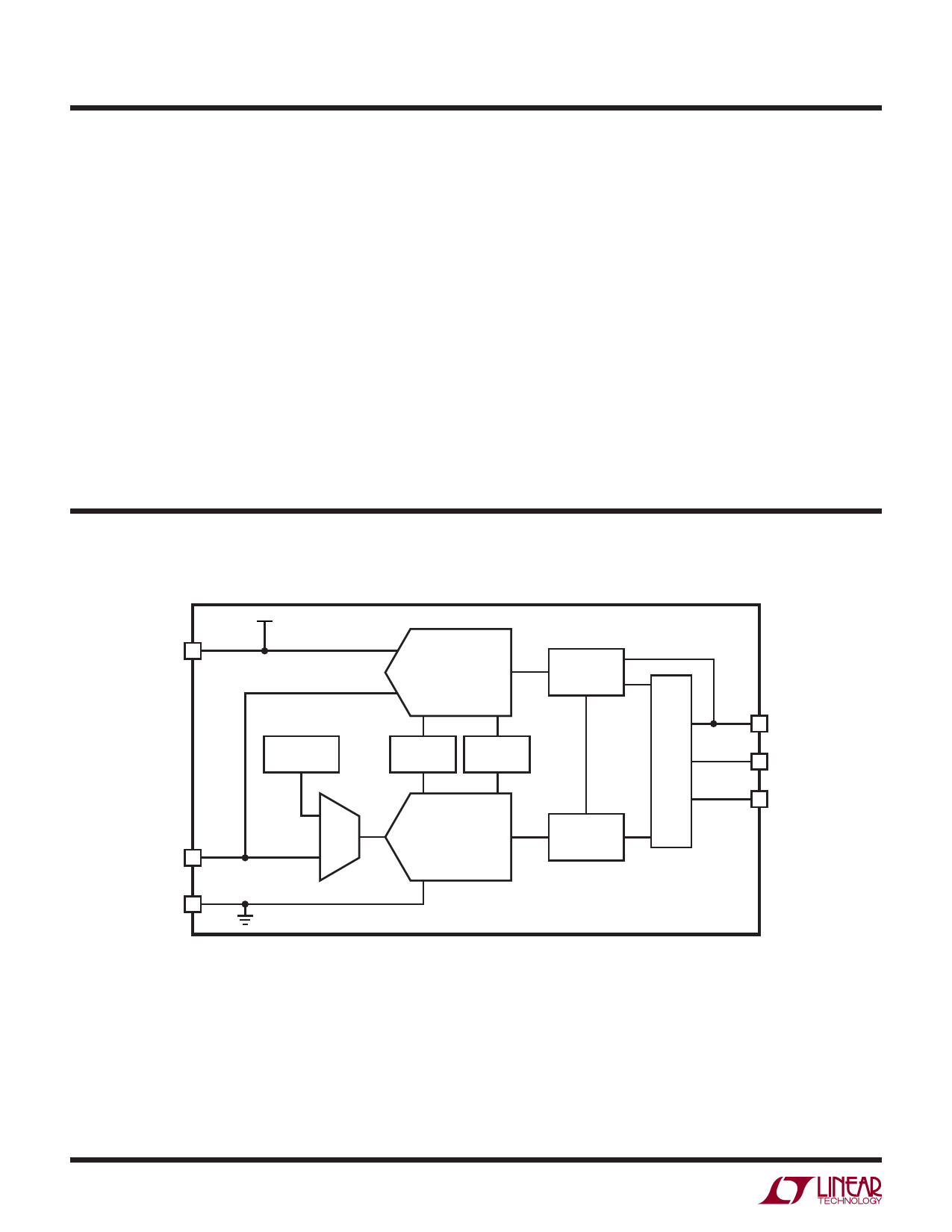
Block Diagram
SENSE+
1
VSUPPLY
TEMPERATURE
SENSOR
MUX
SENSE–
6
GND
2
LTC2942
COULOMB COUNTER
REF
CLK
REFERENCE
GENERATOR
OSCILLATOR
REF+
CLK
IN
ADC
REF–
CC
ACCUMULATED
CHARGE
REGISTER
DATA AND
CONTROL
REGISTERS
AL AL/CC
5
I2C/
SMBus
SCL
3
SDA
4
2942 BD
2942fa
6
Share Link: 