NLX1G11MUTCG View Datasheet(PDF) - ON Semiconductor
Part Name
Description
MFG CO.
NLX1G11MUTCG Datasheet PDF : 7 Pages
| |||
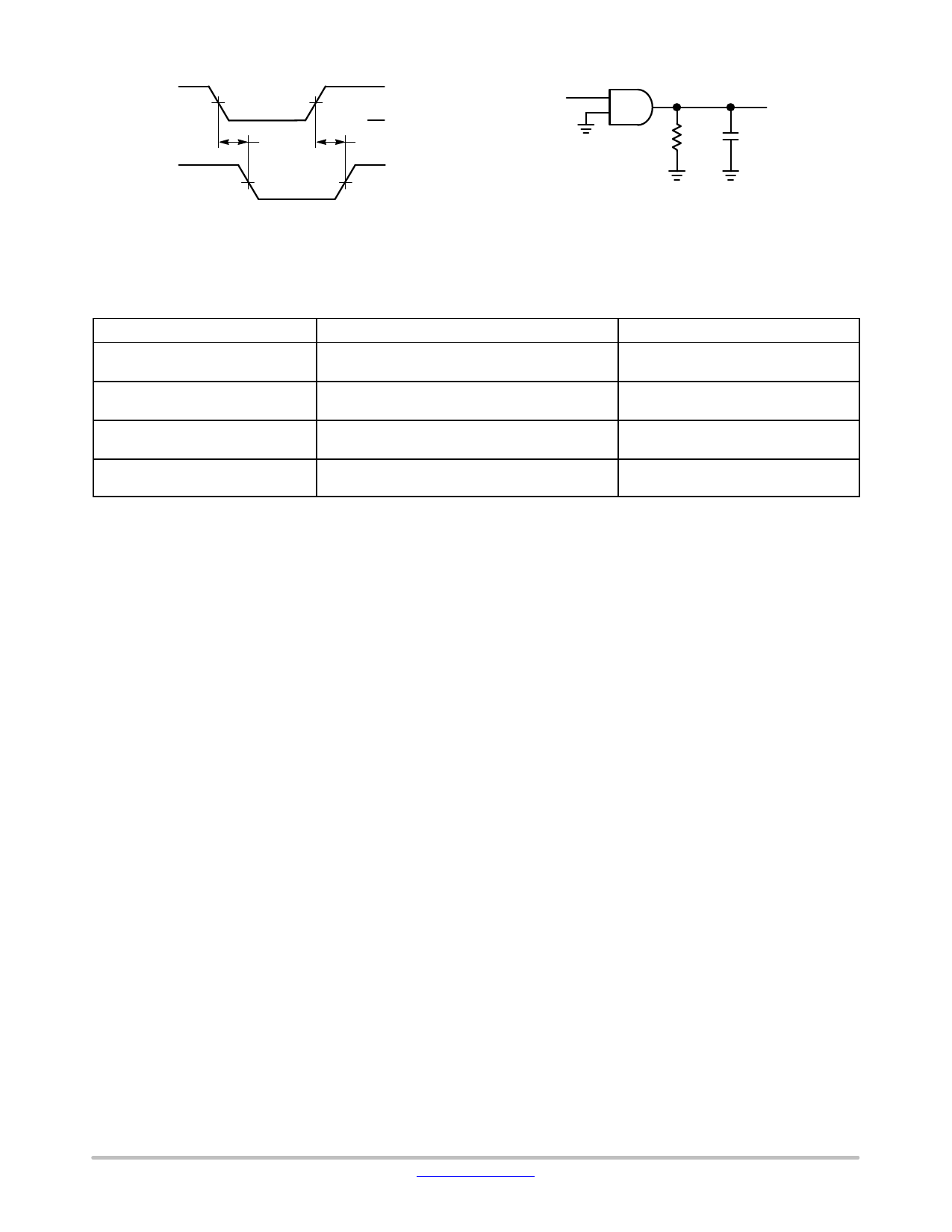
NLX1G11
A and B
50%
tPLH
VCC
GND
tPHL
Y
50% VCC
tR = tF = 2.5 ns, 10% to 90%, f = 1 MHz, tW = 500 ns
Figure 3. Switching Waveforms
INPUT
OUTPUT
RL
CL
A 1 MHz square input wave is recommended
for propagation delay tests
Figure 4. Test Circuit
ORDERING INFORMATION
Device
Package
Shipping†
NLX1G11MUTCG
(In Development)
UDFN6, 1.2 x 1.0, 0.4P
(Pb−Free)
3000 / Tape & Reel
NLX1G11AMUTCG
UDFN6, 1.45 x 1.0, 0.5P
(Pb−Free)
3000 / Tape & Reel
NLVX1G11AMUTCG*
UDFN6, 1.45 x 1.0, 0.5P
(Pb−Free)
3000 / Tape & Reel
NLX1G11CMUTCG
UDFN6, 1.0 x 1.0, 0.35P
(Pb−Free)
3000 / Tape & Reel
†For information on tape and reel specifications, including part orientation and tape sizes, please refer to our Tape and Reel Packaging
Specifications Brochure, BRD8011/D.
*NLV Prefix for Automotive and Other Applications Requiring Unique Site and Control Change Requirements; AEC−Q101 Qualified and PPAP
Capable.
www.onsemi.com
4
Share Link: 