HIP6304CB View Datasheet(PDF) - Intersil
Part Name
Description
MFG CO.
HIP6304CB Datasheet PDF : 14 Pages
| |||
HIP6304
Current Sensing and Balancing
Overview
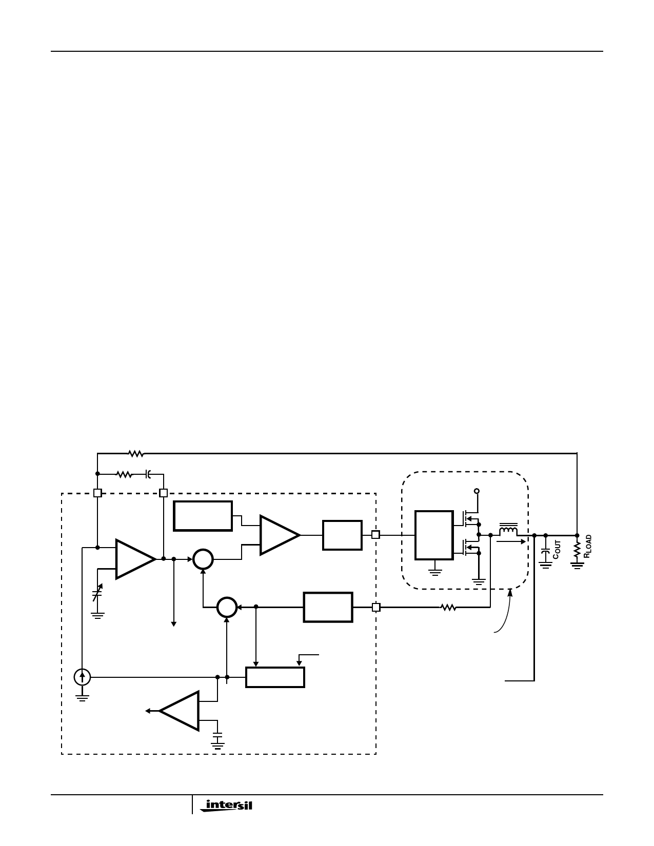
The HIP6304 samples the on-state voltage drop across each
synchronous rectifier FET, Q2, as an indication of the
inductor current in that phase, see Figure 7. Neglecting AC
effects (to be discussed later), the voltage drop across Q2 is
simply rDS(ON) (Q2) x inductor current (IL). Note that IL, the
inductor current, is 1/2 of the total current (ILT).
The voltage at Q2’s drain, the PHASE node, is applied to the
RISEN resistor to develop the IISEN current to the HIP6304
ISEN pin. This pin is held at virtual ground, so the current
through RISEN is IL x rDS(ON)(Q2) / RISEN.
The IISEN current provides information to perform the
following functions:
1. Detection of an over-current condition
2. Reduce the regulator output voltage with increasing load
current (droop)
3. Balance the IL currents in the two phases
Over-Current, Selecting RISEN
The current detected through the RISEN resistor is averaged
with the current detected in the other channel. The averaged
current is compared with a trimmed, internally generated
current, and used to detect an over-current condition.
The nominal current through the RISEN resistor should be
50µA at full output load current, and the nominal trip point for
over-current detection is 165% of that value, or 82.5µA.
Therefore, RISEN = IL x rDS(ON) (Q2) / 50µA.
For a full load of 25A per phase, and an rDS(ON) (Q2) of
4mΩ, RISEN = 2kΩ .
The over-current trip point would be 165% of 25A, or ~ 41A
per phase. The RISEN value can be adjusted to change the
over-current trip point, but it is suggested to stay within ±25%
of nominal.
Droop, Selection of RIN
The average of the currents detected through the RISEN
resistors is also steered to the FB pin. There is no DC return
path connected to the FB pin except for RIN, so the average
current creates a voltage drop across RIN. This drop increases
the apparent VCORE voltage with increasing load current,
causing the system to decrease VCORE to maintain balance at
the FB pin. This is the desired “droop” voltage used to maintain
VCORE within limits under transient conditions.
With a high dv/dt load transient, typical of high performance
microprocessors, the largest deviations in output voltage
occur at the leading and trailing edges of the load transient. In
order to fully utilize the output-voltage tolerance range, the
output voltage is positioned in the upper half of the range
when the output is unloaded and in the lower half of the range
when the controller is under full load. This droop
compensation allows larger transient voltage deviations and
thus reduces the size and cost of the output filter components.
RIN
FB
RFB Cc
COMP
ERROR
AMPLIFIER
-
+
SAWTOOTH
GENERATOR
CORRECTION
+
-
HIP6304
COMPARATOR
-
PWM
+
CIRCUIT
PWM
REFERENCE
DAC
TO OTHER
CHANNEL
DIFFERENCE
+
-
AVERAGING
CURRENT
SENSING
CURRENT
SENSING
FROM
OTHER
CHANNEL
ISEN
TO OVER
+
CURRENT
TRIP
-
COMPARATOR
REFERENCE
VIN
Q1 L01
HIP6601
Q2
IL
PHASE
RISEN
ONLY ONE OUTPUT
STAGE SHOWN
INDUCTOR
CURRENT
FROM
OTHER
CHANNEL
VCORE
FIGURE 7. SIMPLIFIED FUNCTIONAL BLOCK DIAGRAM SHOWING CURRENT AND VOLTAGE SAMPLING
9
Share Link: 