ATF-521P8-BLK View Datasheet(PDF) - HP => Agilent Technologies
Part Name
Description
MFG CO.
ATF-521P8-BLK
HP => Agilent Technologies
ATF-521P8-BLK Datasheet PDF : 24 Pages
| |||
1 pF
3.9 nH
1.5 pF
RF Input
50 Ohm
.02 λ
110 Ohm
.03 λ
DUT
110 Ohm 50 Ohm
.03 λ
.02 λ
1.5 pF
RF Output
12 nH
47 nH
15 Ohm
2.2 µF
Gate
Supply
2.2 µF
Drain
Supply
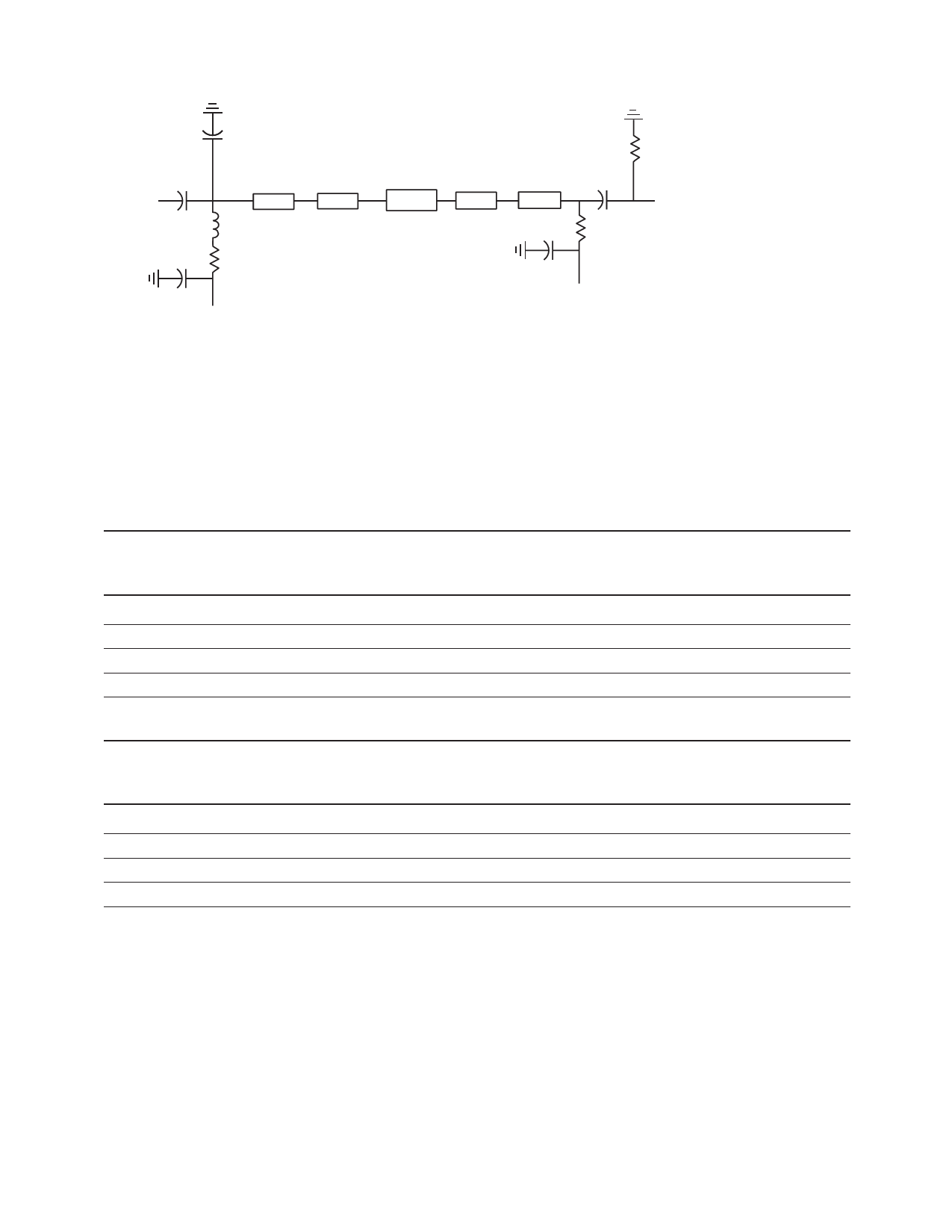
Figure 7. Simplified schematic of production test board. Primary purpose is to show 15 Ohm series resistor placement in
gate supply. Transmission line tapers, tee intersections, bias lines and parasitic values are not shown.
Gamma Load and Source at Optimum OIP3 and P1dB Tuning Conditions
The device’s optimum OIP3 and P1dB measurements were determined using a Maury load pull system at
4.5V, 200 mA quiesent bias:
Freq
(GHz)
0.9
2
2.4
3.9
Gamma Source
Mag
Ang (deg)
0.413
0.368
0.318
0.463
10.5
162.0
169.0
-134.0
Optimum OIP3
Gamma Load
OIP3
Mag
Ang (deg) (dBm)
0.314
179.0
42.7
0.538
-176.0
42.5
0.566
-169.0
42.0
0.495
-159.0
40.3
Gain
(dB)
16.0
15.8
14.1
9.6
P1dB
PAE
(dBm)
(%)
27.0
54.0
27.5
55.3
27.4
53.5
27.3
43.9
Freq
(GHz)
0.9
2
2.4
3.9
Gamma Source
Mag
Ang (deg)
0.587
0.614
0.649
0.552
12.7
126.1
145.0
-162.8
Optimum P1dB
Gamma Load
OIP3
Mag
Ang (deg) (dBm)
0.613
-172.1
39.1
0.652
-172.5
39.5
0.682
-171.5
40.0
0.670
-151.2
38.1
Gain
(dB)
14.5
12.9
12.0
9.6
P1dB
PAE
(dBm)
(%)
29.3
49.6
29.3
49.5
29.4
46.8
27.9
39.1
4
Share Link: 