2N4919G View Datasheet(PDF) - ON Semiconductor
Part Name
Description
MFG CO.
2N4919G Datasheet PDF : 5 Pages
| |||
2N4918 − 2N4920* Series
Preferred Device
Medium−Power Plastic PNP
Silicon Transistors
These medium−power, high−performance plastic devices are
designed for driver circuits, switching, and amplifier applications.
Features
• Pb−Free Package is Available**
• Low Saturation Voltage − VCE(sat) = 0.6 Vdc (Max) @ IC = 1.0 A
• Excellent Power Dissipation Due to Thermopad Construction,
PD = 30 W @ TC = 25_C
• Excellent Safe Operating Area
• Gain Specified to IC = 1.0 A
• Complement to NPN 2N4921, 2N4922, 2N4923
MAXIMUM RATINGS
Rating
Symbol
Value
Unit
Collector − Emitter Voltage
VCEO
Vdc
2N4918
40
2N4919
60
2N4920
80
Collector − Base Voltage
VCBO
Vdc
2N4918
40
2N4919
60
2N4920
80
Emitter − Base Voltage
Collector Current − Continuous
(Note 5)
VEBO
5.0
Vdc
IC
1.0
Adc
(Note 6)
3.0
Base Current
Total Power Dissipation @ TA = 25°C
Derate above 25°C
Operating and Storage Junction
Temperature Range
IB
PD
TJ, Tstg
1.0
30
0.24
−65 to +150
Adc
W
W/°C
°C
Maximum ratings are those values beyond which device damage can occur.
Maximum ratings applied to the device are individual stress limit values (not
normal operating conditions) and are not valid simultaneously. If these limits
are exceeded, device functional operation is not implied, damage may occur
and reliability may be affected.
5. The 1.0 A max IC value is based upon JEDEC current gain requirements. The
3.0 A max value is based upon actual current−handling capability of the
device (See Figure 5).
6. Indicates JEDEC Registered Data for 2N4918 Series.
THERMAL CHARACTERISTICS (Note 7)
Characteristic
Symbol
Max
Unit
Thermal Resistance,
Junction−to−Case
qJC
4.16
°C/W
7. Recommend use of thermal compound for lowest thermal resistance.
http://onsemi.com
3.0 A, 40−80 V, 30 W
GENERAL PURPOSE
POWER TRANSISTORS
3
21
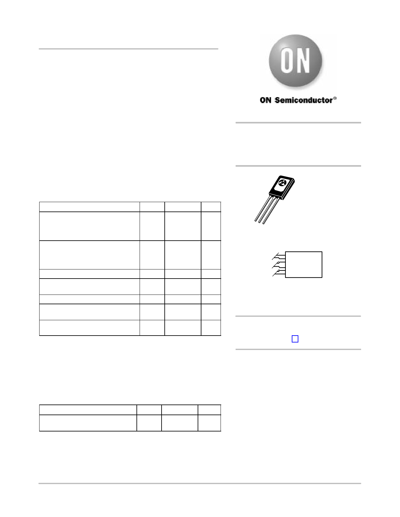
TO−225
CASE 077
STYLE 1
MARKING DIAGRAM
YWW
2N
49xx
xx
= 18, 19, 20
Y
= Year
WW = Work Week
ORDERING INFORMATION
See detailed ordering and shipping information in the package
dimensions section on page 50 of this data sheet.
*Preferred devices are recommended choices for future
use and best overall value.
**For additional information on our Pb−Free strategy and soldering details,
please download the ON Semiconductor Soldering and Mounting Techniques
Reference Manual, SOLDERRM/D.
© Semiconductor Components Industries, LLC, 2004
49
July, 2004 − Rev. 11
Publication Order Number:
2N4918/D
Share Link: 