CS1611A View Datasheet(PDF) - Cirrus Logic
Part Name
Description
MFG CO.
CS1611A Datasheet PDF : 18 Pages
| |||
CS1610A/11A
CS1612A/13A
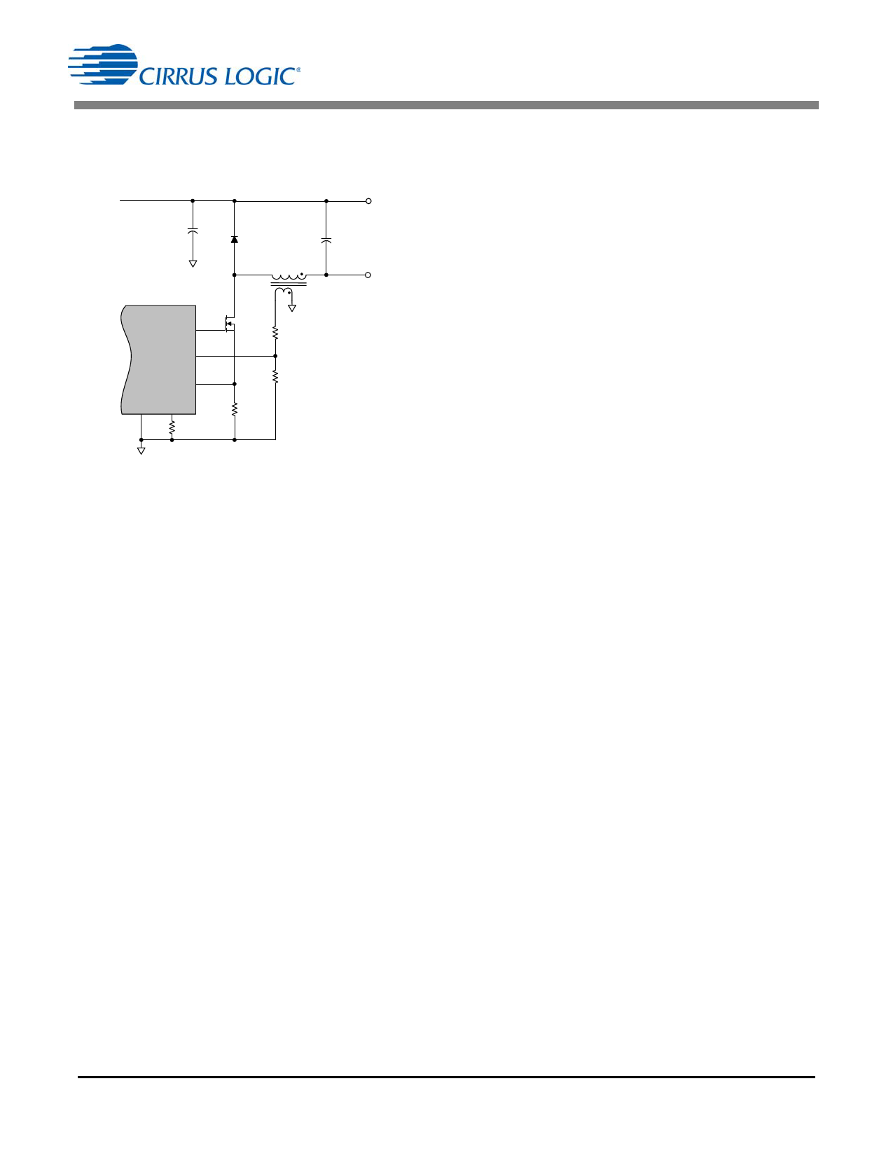
A quasi-resonant buck stage is illustrated in Figure 16. The
buck stage is controlled by measuring current in the buck
inductor and voltage on the auxiliary winding.
VB S T
C8
D8
LED +
C9
LED -
L3
CS1612A/13A
GD 13
FBAUX 15
FBSENSE 11
GND
12
FBGAIN
9
RFB GA IN
Q4
R12
R13
R11
Figure 16. Buck Model
The digital buck algorithm ensures monotonic dimming from
2% to 100% of the dimming range with a linear relationship
between the dimming signal and the LED current.
Quasi-resonant operation is achieved by detecting second
stage inductor demagnetization via an auxiliary winding. The
digital control algorithm rejects line-frequency ripple created
on the second stage input by the front-end boost stage,
resulting in the highest possible LED efficiency and long LED
life.
5.7.1 Auxiliary Winding Configuration
The auxiliary winding is also used for zero-current
detection (ZCD) and overvoltage protection (OVP). The
auxiliary winding is sensed through the FBAUX pin of the IC.
5.7.2 Control Parameters
The second stage control parameters assure the following:
• Line Regulation — The LED current remains constant
despite a ±10% AC line voltage variation.
• Effect of Variation in Transformer Magnetizing
Inductance — The LED current remains constant over
a ±20% variation in magnetizing inductance.
The second stage requires three inputs and generates one
key output. The FBSENSE pin is used to sense the current in
the second stage inductor. When the current reaches a certain
threshold, the gate drive turns ‘OFF’ (output on pin GD). The
sensed current and the FBGain input are used to determine the
total switching period TT. The zero-current detect input on pin
FBAUX is used to determine the demagnetization period T2.
The controller then uses the total switching period TT to
determine gate turn-on time.
The FBGain input is set using resistor RFBGAIN. Resistor
RFBGAIN must be selected to ensure that the switching period
TT is greater than the resonant switching period Tcritical at
maximum output power. See Equation 5:
TT Tcritical = T1 + T2
[Eq. 5]
where,
Tcritical = resonant switching period at max power
T1 = gate turn-on time
T2 = demagnetization time
Total switching period TT is computed for flyback topology
using Equation 6:
TT
IPKFB
T2
F----B-----G----a---i-n-
[Eq. 6]
where,
= dimming factor, proportional to the duty cycle of the
dimmer; between 0 and 1
IPK(FB) = transformer primary winding current
FBGain = constant TT/T2; computed at full load
For buck topology, the switching period TT is computed using
Equation 7:
TT
IPKFB
T1
+
T2
-F----B----G----a---i-n-
[Eq. 7]
where,
= dimming factor, proportional to the duty cycle of the
dimmer, between 0 and 1
IPK(FB) = transformer primary winding current
FBGain = constant TT/(T1 + T2); computed at full load
An appropriate value for resistor RFBGAIN needs to be
selected to provide the correct gain constant FBGain. Resistor
RFBGAIN is calculated using Equation 8:
RFBGAIN = ---F----B----G-6---a2---i-.-n5----k----2--------–----1--
[Eq. 8]
The value of gain constant FBGain also has a bearing on the
linearity of the dimming factor versus the LED current curve
and must be selected using Application Note AN364: Design
Guide for a CS1610 and CS1611 Dimmer-compatible SSL
Circuit and AN372: Design Guide for a CS1612 and CS1613
Dimmer-compatible SSL Circuit.
5.7.3 Output Open Circuit Protection
Output open circuit protection and output overvoltage
protection (OVP) is implemented by monitoring the output
voltage through the transformer auxiliary winding. If the
voltage on the FBAUX pin exceeds OVP threshold VOVP(th) of
1.25V, a fault condition occurs. The IC output is disabled, and
the controller attempts to restart after one second.
12
DS976PP4
Share Link: 