LCK4801 View Datasheet(PDF) - Agere -> LSI Corporation
Part Name
Description
MFG CO.
LCK4801 Datasheet PDF : 10 Pages
| |||
Preliminary Data Sheet
July 2001
LCK4801
Low-Voltage HSTL Differential Clock
Electrical Characteristics (continued)
Table 6. ac Characteristics
VDDA = VDDD = 3.3 V ± 5%, VDDHSTL = 1.7 V—2.1 V, TA = 0 °C—70 °C.
Symbol
Description
Min
Typ
Max
Unit Condition
fref
Input Frequency
fMAX
Maximum Output
Frequency
tsk (o) Skew Error (PCLK)
tjit (0) Phase Jitter (I/O Jitter)
tjit (cc)
Cycle-to-Cycle Jitter
(Full Period)
tjit (1/2 period) Cycle-to-Cycle Jitter
(Half Period)
VDIFout Differential Output
Peak-to-Peak Swing
VX
Differential Output
Crosspoint Voltage
tlock
Maximum PLL Lock Time
—
336
—
—
—
—
0.6
0.68
—
70—125
—
—
1000
MHz
MHZ
—
35
ps
— (output period)/2 —
—
5
%
—
8
%
—
—1
—2
—2
—2,3
—2,4
—
—
V For all HSTL
output pairs.
—
0.9
V For all HSTL
output pairs.
—
10
ms
—
1. When the phase-locked loop is active but in bypass mode, fref maximum is limited by input the buffer; optimum performance is obtained
from PECL input.
2. At differential pair crossover.
3. Full PCLK period.
4. Half PCLK period.
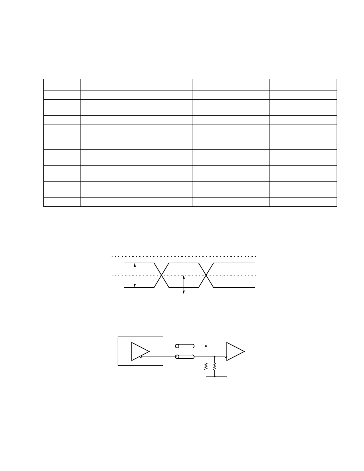
VDIF
VCM
VDDHSTL
VOH
VX
VOL
VSS
Figure 3. HSTL Differential Input Levels
2276 (F)
Z = 50 Ω
OUTPUT
RT = 25 Ω
VTT = VSS (GROUND)
Figure 4. Output Termination and ac Test Reference
2277 (F)
Agere Systems Inc.
7
Share Link: 