CXA3099N View Datasheet(PDF) - Sony Semiconductor
Part Name
Description
MFG CO.
CXA3099N Datasheet PDF : 15 Pages
| |||
CXA3099N
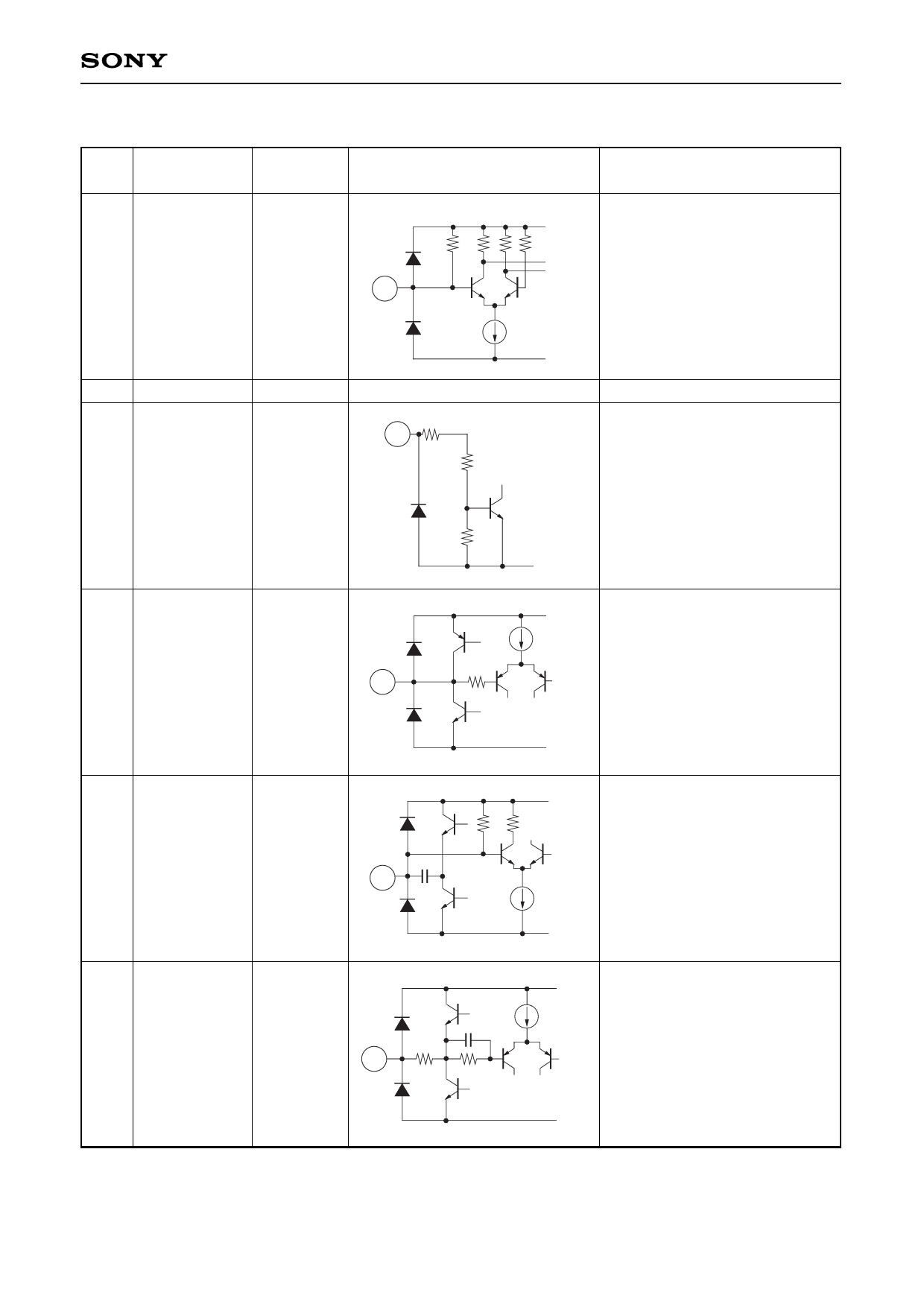
Pin Description
Pin
Symbol
No.
1
IF IN
Pin voltage
1.4 V
Equivalent circuit
20k 20k
VCC
1.5k
1.5k
1
Description
IF limiter amplifier input.
2
GND
3
B.S.
4
FSK REF
5
QUAD
6
DET OUT
—
—
0.2 V
1.4 V
0.2V
72
3
40k
140k
72
4
GND
Ground.
Controls the battery saving.
Setting this pin low suspends the
operation of IC. (Applied voltage
range: –0.5 V to +7.0 V)
GND
VCC
Connects the capacitor that
determines the low cut-off
frequency for the entire system.
GND
5
20p
VCC
22k
20k
Connects the phase shifter of FM
detector circuit.
GND
50p
6
72 55k
VCC
FM detector output.
GND
—3—
Share Link: 