BSP171 View Datasheet(PDF) - Siemens AG
Part Name
Description
MFG CO.
BSP171 Datasheet PDF : 8 Pages
| |||
BSP 171
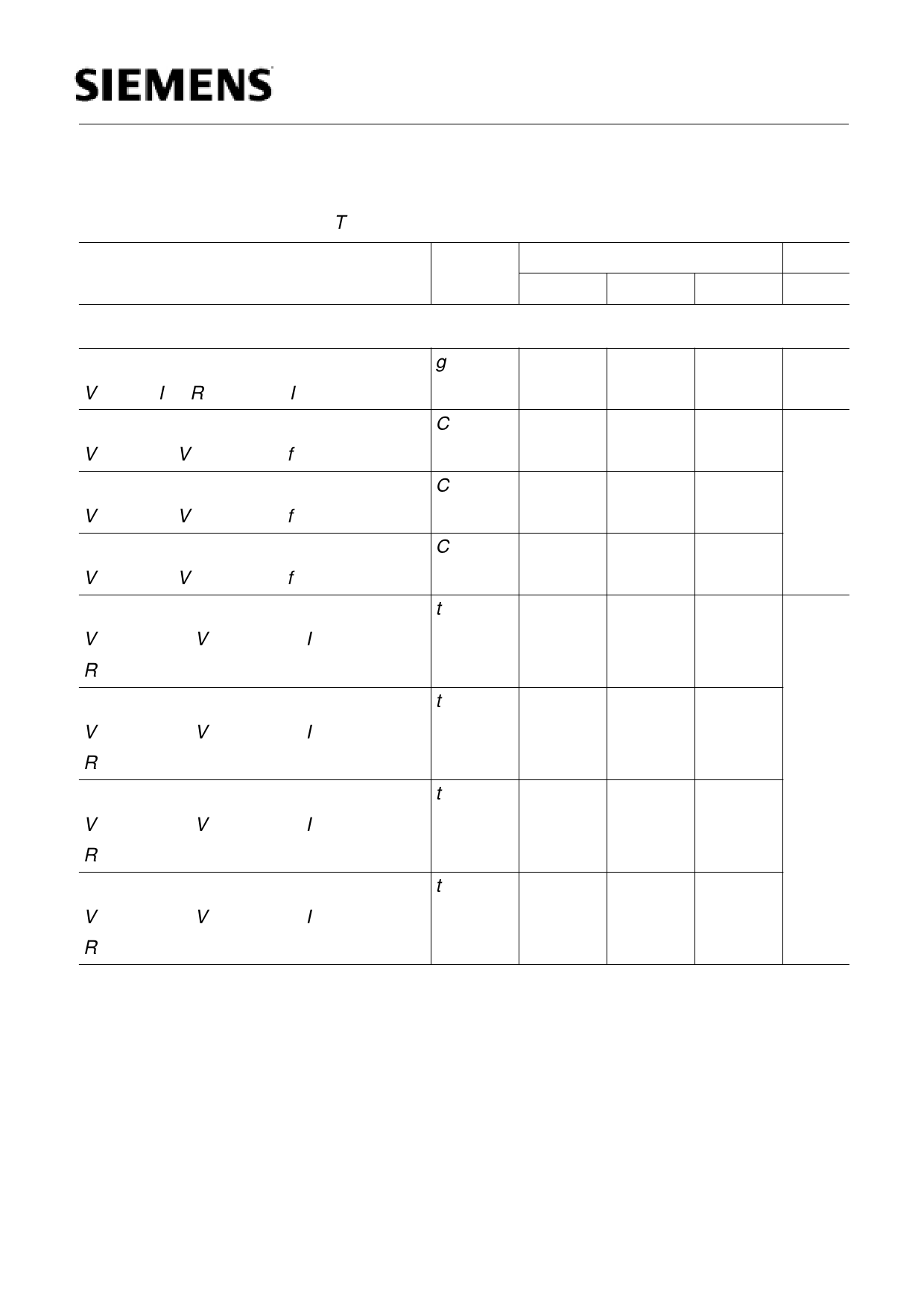
Electrical Characteristics, at Tj = 25°C, unless otherwise specified
Parameter
Symbol
Values
min.
typ.
max.
Dynamic Characteristics
Transconductance
gfs
VDS≥ 2 * ID * RDS(on)max, ID = -1.7 A
1
Input capacitance
Ciss
VGS = 0 V, VDS = -25 V, f = 1 MHz
-
Output capacitance
Coss
VGS = 0 V, VDS = -25 V, f = 1 MHz
-
Reverse transfer capacitance
Crss
VGS = 0 V, VDS = -25 V, f = 1 MHz
-
Turn-on delay time
td(on)
VDD = -30 V, VGS = -10 V, ID = -0.3 A
RGS = 50 Ω
-
Rise time
tr
VDD = -30 V, VGS = -10 V, ID = -0.3 A
RGS = 50 Ω
-
Turn-off delay time
td(off)
VDD = -30 V, VGS = -10 V, ID = 0.3 A
RGS = 50 Ω
-
Fall time
tf
VDD = -30 V, VGS = -10 V, ID = -0.3 A
RGS = 50 Ω
-
1.55 -
720
960
290
435
120
180
16
25
70
105
230
310
280
375
Unit
S
pF
ns
Semiconductor Group
3
18/02/1997
Share Link: 