TDA3601Q View Datasheet(PDF) - Philips Electronics
Part Name
Description
MFG CO.
TDA3601Q Datasheet PDF : 12 Pages
| |||
Philips Semiconductors
Multiple output voltage regulators
Product specification
TDA3601Q
TDA3601AQ
FEATURES
• Six fixed voltage regulators
• Three microprocessor-controlled regulators
• Two VP-state controlled regulators
• One fixed voltage regulator (can operate during load
dump or thermal shutdown)
• VP1 supply pin (low current pin)
• VP2 supply pin (high current pin)
• RESET output (TDA3601Q) or RESET output
(TDA3601AQ)
• Internally fixed timer of 100 µs
• Externally fixed delay timer
• High ripple rejection
• Flexible leads.
PROTECTION
• Current limit protection for regulator 1
• Foldback current limit protection (regulators 2 to 6)
• Load dump protection
• Thermal protection
• Regulator outputs DC short-circuit-safe to ground,
VP and other regulator outputs
• Capable of handling high energy on any of the
output pins
• Reverse polarity safe.
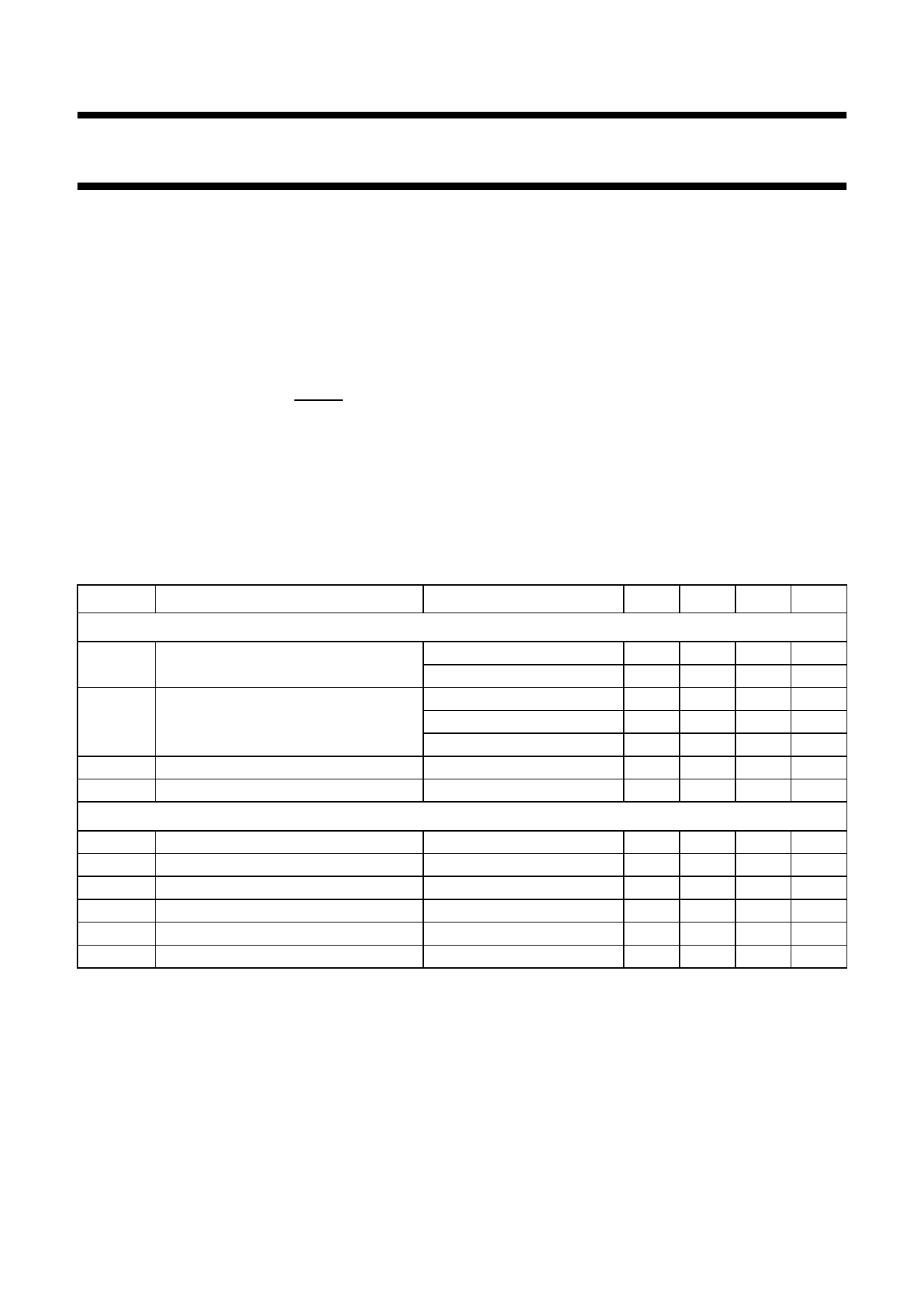
QUICK REFERENCE DATA
SYMBOL
PARAMETER
CONDITIONS
Entire device
VP1
supply voltage range
VP2
supply voltage range
I1tot
total quiescent current, VP1
Tc
crystal temperature
operating
load dump; notes 1 and 2
operating
non-operating
load dump; note 1
VP2 = 0; note 3
Voltage regulators
VR1
output voltage regulator 1
VR2
output voltage regulator 2
VR3
output voltage regulator 3
VR4
output voltage regulator 4
VR5
output voltage regulator 5
VR6
output voltage regulator 6
0.5 mA ≤ IR1 ≤ 20 mA
5 mA ≤ IR2 ≤ 200 mA
5 mA ≤ IR3 ≤ 150 mA
5 mA ≤ IR4 ≤ 150 mA
5 mA ≤ IR5 ≤ 200 mA
5 mA ≤ IR6 ≤ 200 mA
Notes
1. Load dump, during 50 ms, tr > 2.5 ms.
2. Regulator 1 operating, 0.5 mA ≤ IR1 ≤ 20 mA.
3. VP1 = 13.2 V; VP2 = R4-sel = R5-sel = 0; IR1 = 0.
MIN. TYP. MAX. UNIT
11
13.2 18
V
−
−
50
V
11
13.2 18
V
−
−
30
V
−
−
50
V
−
1
1.4 mA
−
−
150 °C
4.75 5
5.25 V
1.9 2.1 2.3 V
4.75 5
5.25 V
9
9.5 10
V
9
9.5 10
V
9.3 9.75 10.2 V
1995 Dec 13
2
Share Link: 