MC14025B(2014) View Datasheet(PDF) - ON Semiconductor
Part Name
Description
MFG CO.
MC14025B Datasheet PDF : 11 Pages
| |||
MC14001B Series
B−SERIES GATE SWITCHING TIMES
SWITCHING CHARACTERISTICS (Note 5) (CL = 50 pF, TA = 25_C)
Characteristic
VDD
Symbol
Vdc
Typ
Min
(Note 6)
Max
Unit
Output Rise Time, All B−Series Gates
tTLH = (1.35 ns/pF) CL + 33 ns
tTLH = (0.60 ns/pF) CL + 20 ns
tTLH = (0.40 ns/PF) CL + 20 ns
tTLH
ns
5.0
−
100
200
10
−
50
100
15
−
40
80
Output Fall Time, All B−Series Gates
tTHL = (1.35 ns/pF) CL + 33 ns
tTHL = (0.60 ns/pF) CL + 20 ns
tTHL = (0.40 ns/pF) CL + 20 ns
tTHL
ns
5.0
−
100
200
10
−
50
100
15
−
40
80
Propagation Delay Time
MC14001B, MC14011B only
tPLH, tPHL = (0.90 ns/pF) CL + 80 ns
tPLH, tPHL = (0.36 ns/pF) CL + 32 ns
tPLH, tPHL = (0.26 ns/pF) CL + 27 ns
All Other 2, 3, and 4 Input Gates
tPLH, tPHL = (0.90 ns/pF) CL + 115 ns
tPLH, tPHL = (0.36 ns/pF) CL + 47 ns
tPLH, tPHL = (0.26 ns/pF) CL + 37 ns
8−Input Gates (MC14068B, MC14078B)
tPLH, tPHL = (0.90 ns/pF) CL + 155 ns
tPLH, tPHL = (0.36 ns/pF) CL + 62 ns
tPLH, tPHL = (0.26 ns/pF) CL + 47 ns
tPLH, tPHL
ns
5.0
−
125
250
10
−
50
100
15
−
40
80
5.0
−
160
300
10
−
65
130
15
−
50
100
5.0
−
200
350
10
−
80
150
15
−
60
110
5. The formulas given are for the typical characteristics only at 25_C.
6. Data labelled “Typ” is not to be used for design purposes but is intended as an indication of the IC’s potential performance.
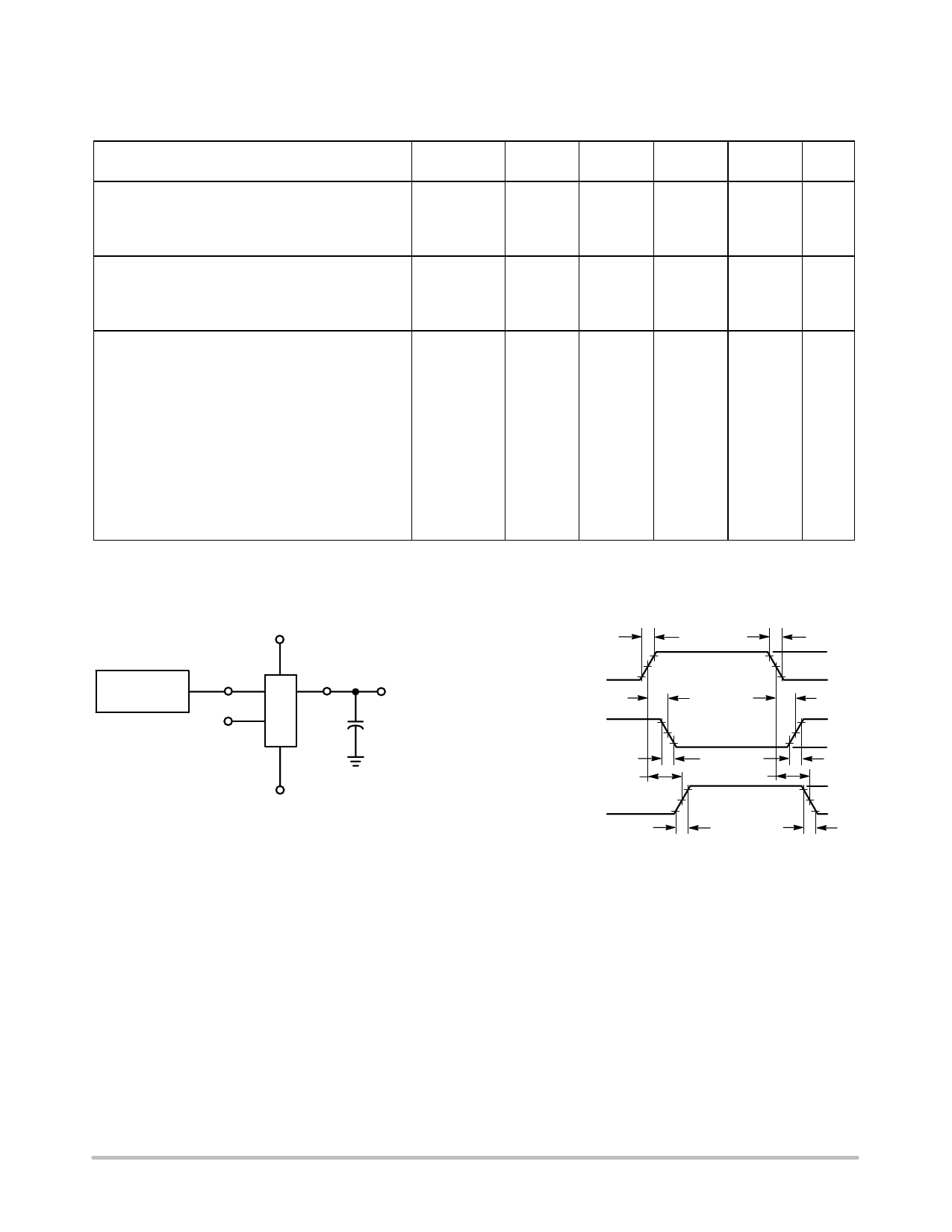
PULSE
GENERATOR
14 VDD
INPUT
*
OUTPUT
CL
7 VSS
*All unused inputs of AND, NAND gates must be connected to VDD.
All unused inputs of OR, NOR gates must be connected to VSS.
20 ns
20 ns
INPUT
90%
50%
VDD
10%
0V
tPHL
tPLH
OUTPUT
INVERTING tTHL
90%
50%
10%
tTLH
VOH
VOL
tPLH
OUTPUT
tPHL
90%
VOH
NON-INVERTING
50%
10%
VOL
tTLH
tTHL
Figure 1. Switching Time Test Circuit and Waveforms
http://onsemi.com
4
Share Link: 