L6204D View Datasheet(PDF) - STMicroelectronics
Part Name
Description
MFG CO.
L6204D Datasheet PDF : 12 Pages
| |||
L6204
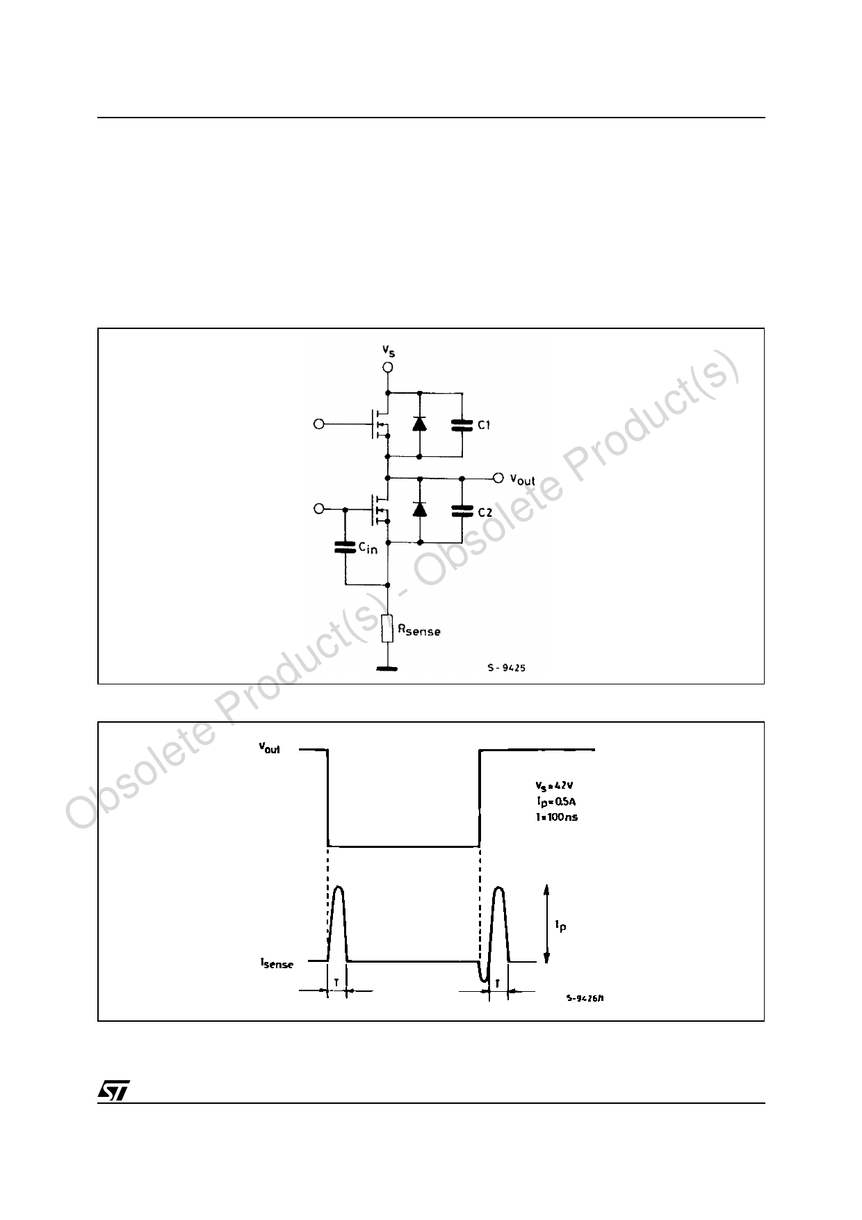
CROSS CONDUCTION
Although the device guarantees the absence of cross-conduction, the presence of the intrinsic diodes in
the POWER DMOS structure causes the generation of current spikes on the sensing terminals.
This is due to charge-discharge phenomena in the capacitors C1 & C2 associated with the drain source
junctions (fig. 1). When the output switches from high to low, a current spike is generated associated with
the capacitor C1. On the low-to-high transition a spike of the same polarity is generated by C2, preceded
by a spike of the opposite polarity due to the charging of the input capacity of the lower POWER DMOS
transistor (see fig. 2).
Figure 1. Intrinsic Structures in the POWER MOS Transistors
Obsolete Product(s) - Obsolete Product(s) Figure 2. Current Typical Spikes on the Sensing Pin
5/12
Share Link: 