MC74HC112DT View Datasheet(PDF) - Motorola => Freescale
Part Name
Description
MFG CO.
MC74HC112DT Datasheet PDF : 6 Pages
| |||
MOTOROLA
SEMICONDUCTOR TECHNICAL DATA
Dual J-K Flip-Flop with
Set and Reset
High–Performance Silicon–Gate CMOS
The MC74HC112 is identical in pinout to the LS112. The device inputs are
compatible with standard CMOS outputs; with pullup resistors, they are
compatible with LSTTL outputs.
Each flip–flop is negative–edge clocked and has active–low asynchro-
nous Set and Reset inputs.
The HC112 is identical in function to the HC76, but has a different pinout.
• Output Drive Capability: 10 LSTTL Loads
• Outputs Directly Interface to CMOS, NMOS, and TTL
• Operating Voltage Range: 2 to 6 V
• Low Input Current: 1 µA
• High Noise Immunity Characteristic of CMOS Devices
• In Compliance with the Requirements Defined by JEDEC Standard
No. 7A
• Similar in Function to the LS112 Except When Set and Reset are Low
Simultaneously
• Chip Complexity: 100 FETs or 25 Equivalent Gates
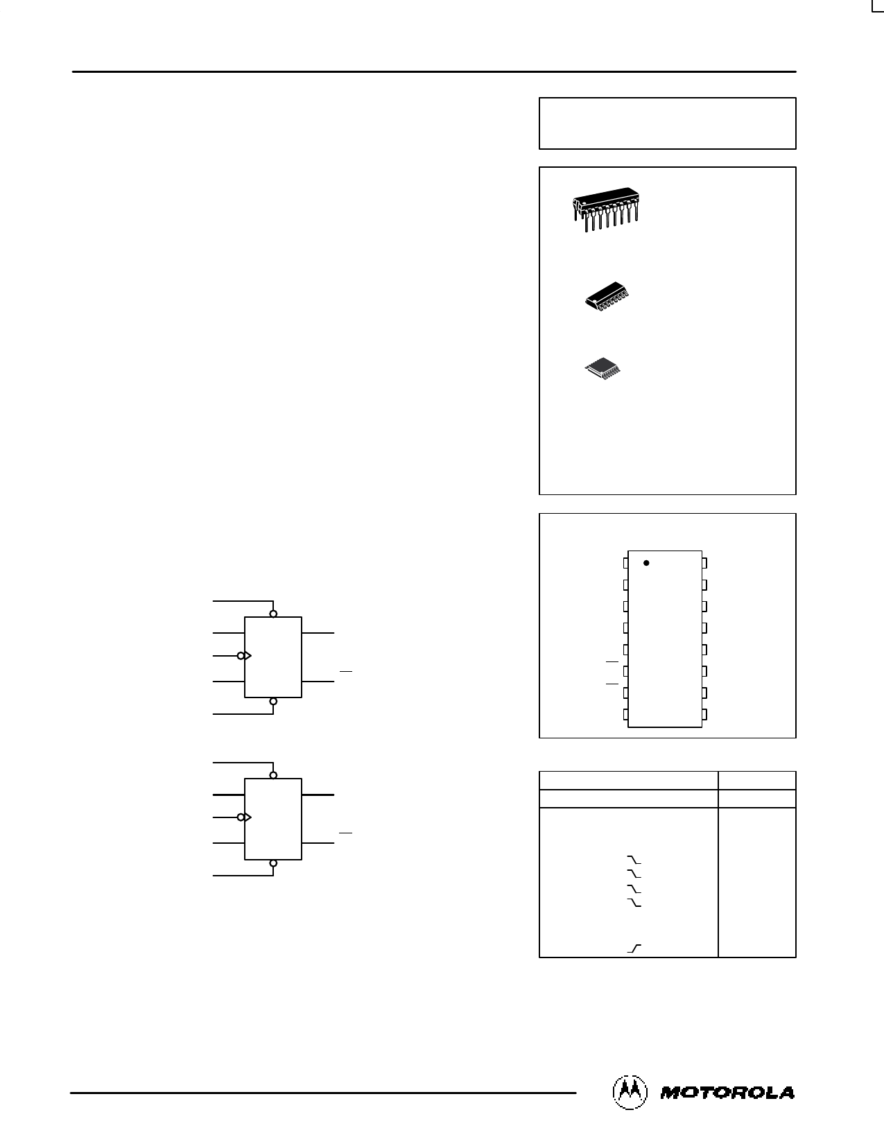
MC74HC112
16
1
N SUFFIX
PLASTIC PACKAGE
CASE 648–08
16
1
D SUFFIX
SOIC PACKAGE
CASE 751B–05
16
1
DT SUFFIX
TSSOP PACKAGE
CASE 948F–01
ORDERING INFORMATION
MC74HCXXXN
MC74HCXXXD
MC74HCXXXDT
Plastic
SOIC
TSSOP
LOGIC DIAGRAM
SET 1 4
K1 2
CLOCK 1 1
J1 3
RESET 1 15
5 Q1
6 Q1
SET 2 10
K2 12
CLOCK 2 13
J2 11
RESET 2 14
PIN 16 = VCC
PIN 8 = GND
9 Q2
7 Q2
PIN ASSIGNMENT
CLOCK 1 1
K1 2
J1 3
SET 1 4
Q1 5
Q1 6
Q2 7
GND 8
16 VCC
15 RESET 1
14 RESET 2
13 CLOCK 2
12 K2
11 J2
10 SET 2
9 Q2
FUNCTION TABLE
Inputs
Set Reset Clock J K
Outputs
QQ
L
H
XXX
HL
H
L
XXX
LH
L
L
XXX
L* L*
H
H
L L No Change
H
H
LH
LH
H
H
HL
HL
H
H
HH
Toggle
H
H
L X X No Change
H
H
H X X No Change
H
H
X X No Change
* Both outputs will remain low as long as Set and
Reset are low, but the output states are unpre-
dictable if Set and Reset go high simultaneously.
10/95
© Motorola, Inc. 1995
1
REV 6
Share Link: 