74ALVC162834A View Datasheet(PDF) - NXP Semiconductors.
Part Name
Description
MFG CO.
74ALVC162834A
NXP Semiconductors.
74ALVC162834A Datasheet PDF : 15 Pages
| |||
Nexperia
74ALVC162834A
18-bit registered driver with inverted register enable and 30 Ω termination resistors; 3-state
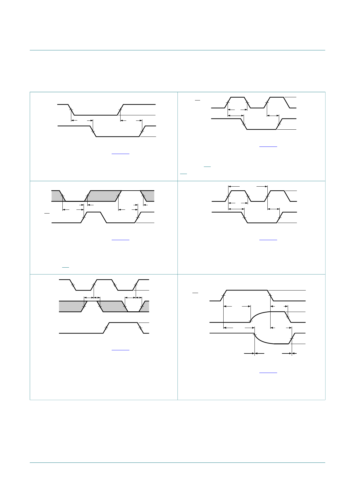
10.1 Waveforms and test circuit
An input
Yn output
VM
tPHL
VM
tPLH
VI
GND
VOH
VOL
002aac726
Measurement points are given in Table 8.
VOL and VOH are typical voltage output levels that occur with
the output load.
Figure 5. Input (An) to output (Yn) propagation delay
LE input
Yn output
VM
tw
tPHL
VM
VM
tPLH
VI
GND
VOH
VOL
002aac727
Measurement points are given in Table 8.
VOL and VOH are typical voltage output levels that occur with
the output load.
Figure 6. LE input pulse width,
LE input to Yn output propagation delays
An
input
LE
input
VM
tsu
th
VM
VM
tsu
VI
GND
th
VI
VM
GND
002aac728
Measurement points are given in Table 8.
The shaded areas indicate when the input is permitted to
change for predictable output performance.
CP input
Yn output
1 / fmax
VM
tw
tPHL
VM
VM
tPLH
VI
GND
VOH
VOL
002aac729
Measurement points are given in Table 8.
VOL and VOH are typical voltage output levels that occur with
the output load.
Figure 7. Data set-up and hold times,
An input to LE input
Figure 8. CP to Yn propagation delays, clock pulse width
and maximum clock frequency
CP
input
An
input
VM
tsu th
tsu th
VI
GND
VI
GND
Yn
output
VOH
VOL
002aac730
Measurement points are given in Table 8.
VOL and VOH are typical voltage output levels that occur with
the output load.
The shaded areas indicate when the input is permitted to
change for predictable output performance.
Figure 9. Data set-up and hold times,
An input to CP input
OE input
output
LOW-to-OFF
OFF-to-LOW
output
HIGH-to-OFF
OFF-to-HIGH
VM
tPLZ
tPHZ
outputs
enabled
VI
tPZL
VX
VY
tPZH
outputs
disabled
GND
VCC
VM
VOL
VOH
VM
GND
outputs
enabled
002aac731
Measurement points are given in Table 8.
VOL and VOH are typical voltage output levels that occur with
the output load.
Figure 10. 3-state enable and disable times
74ALVC162834A
Product data sheet
All information provided in this document is subject to legal disclaimers.
Rev. 3 — 13 June 2017
© Nexperia B.V. 2017. All rights reserved.
9 / 15
Share Link: 