M74HC123F1R View Datasheet(PDF) - STMicroelectronics
Part Name
Description
MFG CO.
M74HC123F1R Datasheet PDF : 14 Pages
| |||
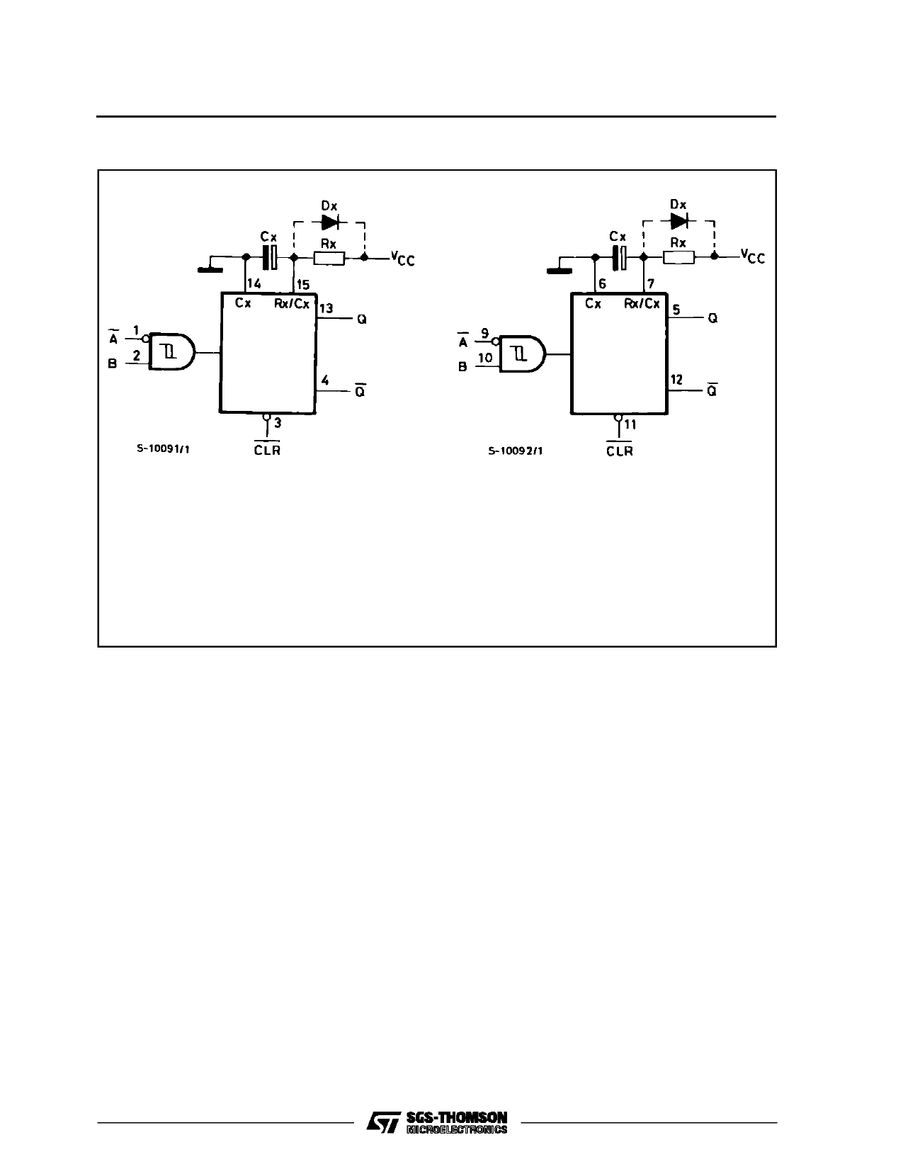
BLOCK DIAGRAM
M54/M74HC123/123A
Note :
(1) Cx, Rx, Dx are external components.
(2) Dx is a clamping diode.
The external capacitor is charged to VCC inthe stand-by state, i.e. no trigger. When the supply voltage is turned off Cx is discharged mainly
through an internal parasitic diode (see figures). If Cx is sufficiently large and VCC decreases rapidy, there will be some possibility of da-
maging the I.C. with a surge current or latch-up. If the voltage supply filter capacitor is large enough and VCC decrease slowly, the surge
current is automatically limited and damage the I.C. is avoided. The maximum forward current of the parasitic diode is approximately 20
mA. In cases where Cx is large the time taken for the supply voltage to fall to 0.4 VCC can be calculated as follows :
tf ≥ (VCC – 0.7) ⋅ Cx/20mA
In cases where tf is too short an external clamping diode is required to protect the I.C. from the surge current.
FUNCTIONAL DESCRIPTION
STAND-BY STATE
The external capacitor, Cx, is fully charged to VCC
in the stand-by state. Hence, before triggering, tran-
sistor Qp and Qn (connected to the Rx/Cx node) are
both turned-off. The two comparators that control
the timing and the two reference voltage sources
stop operating. The total supply current is therefore
only leakage current.
TRIGGER OPERATION
Triggering occurs when :
1 st) A is ”low” and B has a falling edge ;
2 nd) B is ”high” and A has a rising edge ;
3 rd) A is low and B is high and C1 has a rising edge.
After the multivibrator has been retriggered com-
parator C1 and C2 start operating and Qn is turned
on. Cx then discharges through Qn. The voltage at
the node R/C external falls.
When it reaches VREFL the output of comparator C1
becomes low. This in turn resets the flip-flop and Qn
is turned off.
At this point C1 stops functioning but C2 continues
to operate.
The voltage at R/C external begins to rise with a time
constant set by the external components Rx, Cx.
Triggering the multivibrator causes Q to go high after
internal delay due to the flip-flop and the gate. Q re-
mains high until the voltage at R/C external rises
again to VREFH. At this point C2 output goes low and
O goes low. C2 stop operating. That means that
after triggering when the voltage R/C external re-
turns to VREFH the multivibrator has returned to its
MONOSTABLE STATE. In the case where Rx ⋅ Cx
are large enough and the discharge time of the ca-
pacitor and the delay time in the I.C. can be ignored,
the width of the output pulse tw (out) is as follows :
tW(OUT) = 0.46 Cx ⋅ Rx (HC123)
tW(OUT) = Cx ⋅ Rx (HC123A)
3/14
Share Link: 