AD7366 View Datasheet(PDF) - Analog Devices
Part Name
Description
MFG CO.
AD7366 Datasheet PDF : 17 Pages
| |||
AD7366
Preliminary Technical Data
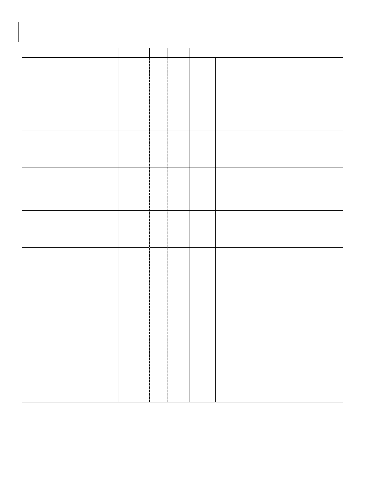
Parameter
REFERENCE INPUT/OUTPUT
Reference Output Voltage4
Reference Input Voltage Range
DC Leakage Current
Input Capacitance
VREFA, VREFB Output Impedance
Reference Temperature
Coefficient
VREF Noise
LOGIC INPUTS
Input High Voltage, VINH
Input Low Voltage, VINL
Input Current, IIN
Input Capacitance, CIN3
LOGIC OUTPUTS
Output High Voltage, VOH
Output Low Voltage, VOL
Floating State Leakage Current
Floating State Output
Capacitance3
CONVERSION RATE
Conversion Time
Track/Hold Acquisition Time3
Throughput Rate
POWER REQUIREMENTS
VCC
VDD
VSS
VDRIVE
Normal Mode (Static)
IDD
ISS
ICC
Normal Mode (Operational)
IDD
ISS
ICC
Shut-Down Mode
IDD
ISS
ICC
Power Dissipation
Normal Mode (Operational)
Shut-Down
Shut-Down
1 Temperature range is −40°C to +85°C
2 See Terminology section.
Min
Typ Max Unit Test Conditions/ Comments
2.5
2.5
+2.5
3.0
±1
25
8
20
10
20
0.7× VDRIVE
0.8
±1
5
V
V
µA
pF
Ω
ppm/°C
±0.2% max @ 25°C
External reference applied to Pin VREFA/Pin VREFB
ppm/°C
µVRMS
V min
V max
µA max
pF typ
VIN = 0 V or VDRIVE
VDRIVE − 0.2
V
0.4
V
±1
µA
10
pF
4.75
+11.5
-16.5
2.7
610 ns
140 ns
Full-scale step input;
1.12
MSPS
For 4.75V≤VDRIVE≤5.25V, fSCLK = 48MHz
1
MSPS
For 2.7V≤VDRIVE<4.75V , fSCLK = 35MHz
Digital I/Ps = 0 V or VDRIVE
5.25 V
See Table 6
+16.5 V
See Table 6
-11.5 V
See Table 6
5.25 V
1
µA
1
µA
1.8
mA
925 µA
725 µA
4
mA
VDD = +16.5 V
VSS = −16.5 V
VCC = 5.5 V
fs = 1.12 MSPS
VDD = +16.5 V
VSS = −16.5 V
VCC = 5.25 V, internal reference enabled
1
µA
VDD = +16.5 V
1
µA
VSS = −16.5 V
1
µA
VCC = 5.25 V
48.23 mW
15
µW
38.25 µW
VDD = +16.5V, VSS = −16.5V, VCC = 5.25V
VDD = +5V, VSS = −5V, VCC = 5V
VDD = +16.5V, VSS = −16.5V, VCC = 5.25
Rev. PrG | Page 4 of 17
Share Link: 