AD7813YRU_97 View Datasheet(PDF) - Analog Devices
Part Name
Description
MFG CO.
AD7813YRU_97 Datasheet PDF : 12 Pages
| |||
EXT
INT
t POWER-UP
BUSY
t1
t2
t3
AD7813
/
DB7–DB0
EXT
INT
BUSY
8 MSBs
Figure 13. Mode 1 Operation
t POWER-UP
t1
t3
2 LSBs
/
DB7–DB0
8 MSBs
Figure 14. Mode 2 Operation
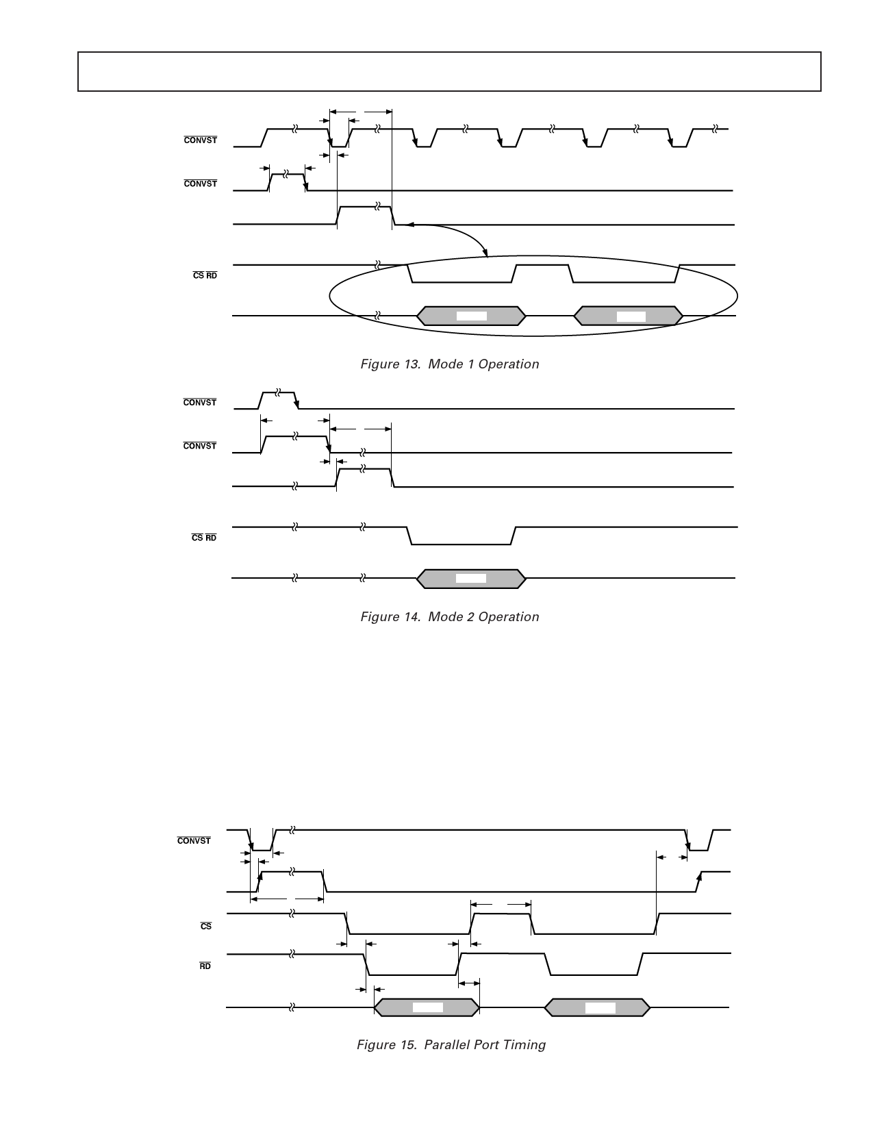
PARALLEL INTERFACE
The parallel interface of the AD7813 is eight bits wide. The
output data buffers are activated when both CS and RD are
logic low. At this point the contents of the data register are
placed on the 8-bit data bus. Figure 15 shows the timing dia-
gram for the parallel port. As previously explained, two succes-
sive read operations must take place in order to access the 10-bit
conversion result. The first read places the 8 MSBs on the data
bus and the second read places the 2 LSBs on the data bus. The
2 LSBs appear on DB7 and DB6, with DB5–DB0 set to logic zero.
Further read operations will access the 8 MSBs and 2 LSBs of
the 10-bit ADC conversion result again. The parallel interface
of the AD7813 is reset when BUSY goes logic high. This feature
allows the AD7813 to be used as an 8-bit converter if the user
only wishes to access the 8 MSBs of the conversion. Care must
be taken to ensure that a read operation does not occur while
BUSY is high. Data read from the AD7813 while BUSY is high
will be invalid. For optimum performance the read operation
should end at least 100 ns (t10) prior to the falling edge of the
next CONVST.
t2
t3
BUSY
t1
t9
t8
DB7–DB0
t4
t6
t5
t7
8 MSBs
Figure 15. Parallel Port Timing
2 MSBs
REV. 0
–9–
Share Link: 