74F2240 View Datasheet(PDF) - Philips Electronics
Part Name
Description
MFG CO.
74F2240 Datasheet PDF : 10 Pages
| |||
Philips Semiconductors
Octal buffers
Product specification
74F2240, 74F2241
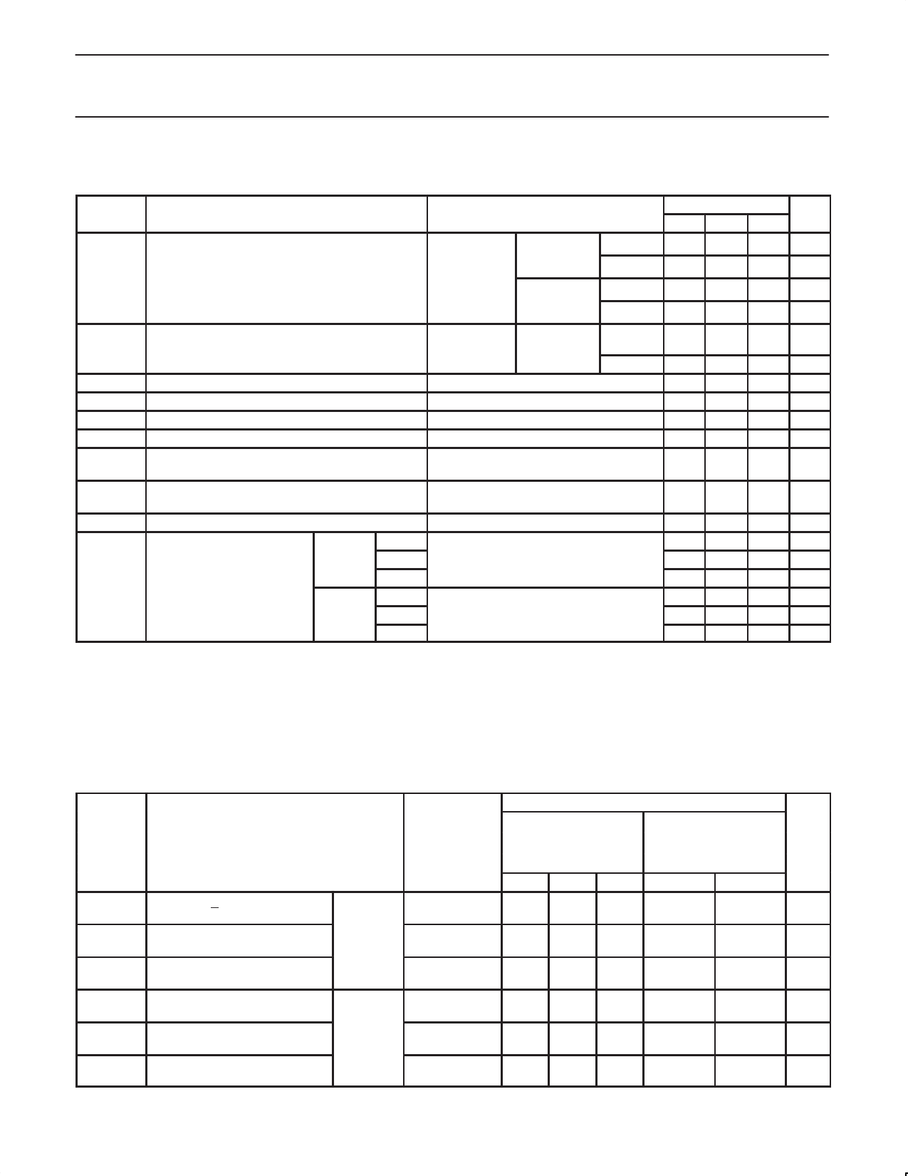
DC ELECTRICAL CHARACTERISTICS
(Over recommended operating free-air temperature range unless otherwise noted.)
SYMBOL
PARAMETER
TEST
CONDITIONS1
LIMITS
UNIT
MIN TYP2 MAX
VOH
High-level output voltage
VCC = MIN,
IOH = –3mA ±10%VC 2.4
V
VIL = MAX,
±5%CVCC 2.7
3.4
V
VIH = MIN
IOH =
±10%VC 2.0
V
–15mA
±5%CVCC 2.0
V
VOL
Low-level output voltage
VIK
II
IIH
IIL
IOZH
Input clamp voltage
Input current at maximum input voltage
High–level input current
Low–level input current
Off–state output current,
high–level voltage applied
VCC = MIN,
VIL = MAX,
IOL = MAX
VIH = MIN,
VCC = MIN, II = IIK
VCC = MAX, VI = 7.0V
VCC = MAX, VI = 2.7V
VCC = MAX, VI = 0.5V
VCC = MAX, VO = 2.7V
±10%VC
C
±5%VCC
0.50 V
0.42 0.50 V
–0.73 -1.2 V
100 µA
20 µA
–0.2 mA
50 µA
IOZL
Off–state output current,
low–level voltage applied
VCC = MAX, VO = 0.5V
–50 µA
IOS
Short–circuit output current3
VCC = MAX
-60
-150 mA
ICCH
25 35 mA
74F2240 ICCL VCC = MAX
53 75 mA
ICC
Supply current (total)
ICCZ
35 45 mA
ICCH
19 30 mA
74F2241 ICCL VCC = MAX
45 65 mA
ICCZ
27 40 mA
NOTES:
1. For conditions shown as MIN or MAX, use the appropriate value specified under recommended operating conditions for the applicable type.
2. All typical values are at VCC = 5V, Tamb = 25°C.
3. Not more than one output should be shorted at a time. For testing IOS, the use of high-speed test apparatus and/or sample-and-hold
techniques are preferable in order to minimize internal heating and more accurately reflect operational values. Otherwise, prolonged shorting
of a high output may raise the chip temperature well above normal and thereby cause invalid readings in other parameter tests. In any
sequence of parameter tests, IOS tests should be performed last.
AC ELECTRICAL CHARACTERISTICS
SYMBOL
PARAMETER
tPLH
tPHL
tPZH
tPZL
tPHZ
tPLZ
tPLH
tPHL
tPZH
tPZL
tPHZ
tPLZ
Propagation delay
Ian, Ibn to Yn
Output enable time
to high or low level
Output disable time
from high or low level
Propagation delay
Ian, Ibn to Yn
Output enable time
to high or low level
Output disable time
from high or low level
74F2240
74F2241
TEST
CONDITION
Waveform 1
Waveform 3
Waveform 4
Waveform 3
Waveform 4
Waveform 2
Waveform 3
Waveform 4
Waveform 3
Waveform 4
LIMITS
Tamb = +25°C
VCC = +5.0V
CL = 50pF, RL = 500Ω
MIN TYP MAX
Tamb = 0°C to +70°C
VCC = +5.0V ± 10%
CL = 50pF, RL = 500Ω
MIN
MAX
3.0
5.0
7.0
2.5
8.0
2.0
3.5
5.5
2.0
6.0
3.0
4.5
7.0
2.5
8.0
3.5
5.0
8.0
3.0
9.0
2.0
3.5
6.5
1.5
7.0
1.0
2.5
5.5
1.0
5.5
3.0
4.5
7.0
2.5
8.0
2.5
4.5
6.5
2.5
7.5
3.0
5.0
7.0
2.0
8.0
3.5
5.5
7.5
3.0
8.5
2.0
4.0
6.0
1.5
7.0
1.5
3.5
6.0
1.0
6.5
UNIT
ns
ns
ns
ns
ns
ns
December 13, 1990
5
Share Link: 