ICS8702BYT View Datasheet(PDF) - Integrated Circuit Systems
Part Name
Description
MFG CO.
ICS8702BYT Datasheet PDF : 12 Pages
| |||
Integrated
Circuit
Systems, Inc.
ICS8702
LOW SKEW ¸1, ¸2
CLOCK GENERATOR
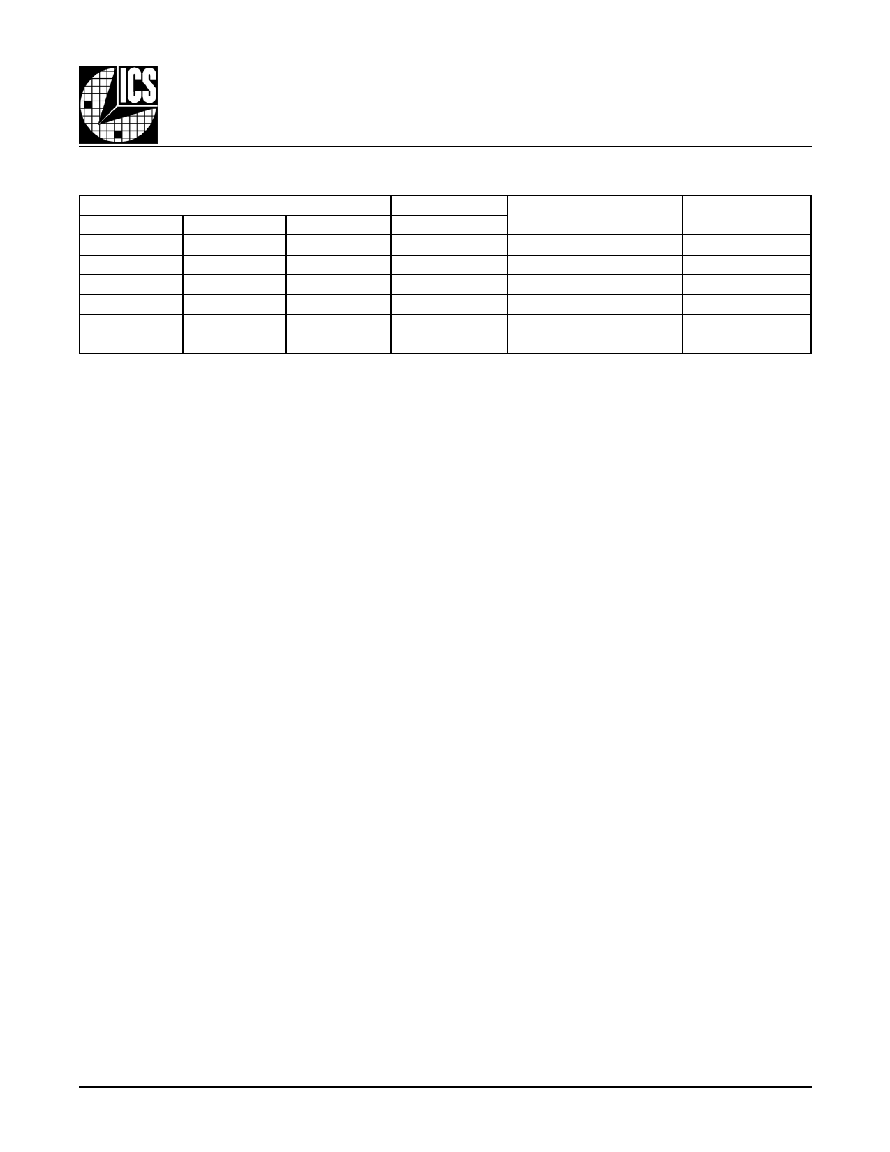
TABLE 3B. CLOCK INPUTS FUNCTION TABLE
nMR/OE
Inputs
CLK
nCLK
Outputs
Qx0 thru Qx4
Input to Output Mode
Polarity
1
0
1
LOW
Differential to Single Ended
Non Inverting
1
1
0
HIGH
Differential to Single Ended
Non Inverting
1
0
Biased; NOTE 1
LOW
Single Ended to Single Ended
Non Inverting
1
1
Biased; NOTE 1
HIGH
Single Ended to Single Ended
Non Inverting
1
Biased; NOTE 1
0
HIGH
Single Ended to Single Ended
Inverting
1
Biased; NOTE 1
1
LOW
Single Ended to Single Ended
Inverting
NOTE 1: Single ended input use requires that one of the differential inputs be biased. The voltage at the biased input sets the switch point for
the single ended input. For LVCMOS input levels the recommended input bias network is a resistor to VDDI, a resistor of equal value to
ground and a 0.1µF capacitor from the input to ground. The resulting switch point is approximately VDD/2 ± 300mV.
ABSOLUTE MAXIMUM RATINGS
Supply Voltage
4.6V
Inputs
Outputs
Ambient Operating Temperature
Storage Temperature
-0.5V to VDD + 0.5V
-0.5V to VDDO + 0.5V
0°C to 70°C
-65°C to 150°C
Stresses beyond those listed under Absolute Maximum Ratings may cause permanent damage to the device. These ratings are stress
specifications only and functional operation of product at these condition or any conditions beyond those listed in the DC Electrical
Characteristics or AC Electrical Characteristics is not implied. Exposure to absolute maximum rating conditions for extended periods may
affect product reliability.
8702
www.icst.com
3
REV. A - AUGUST 7, 2000
Share Link: 