Q67000-S063 View Datasheet(PDF) - Infineon Technologies
Part Name
Description
MFG CO.
Q67000-S063 Datasheet PDF : 8 Pages
| |||
SN 7002
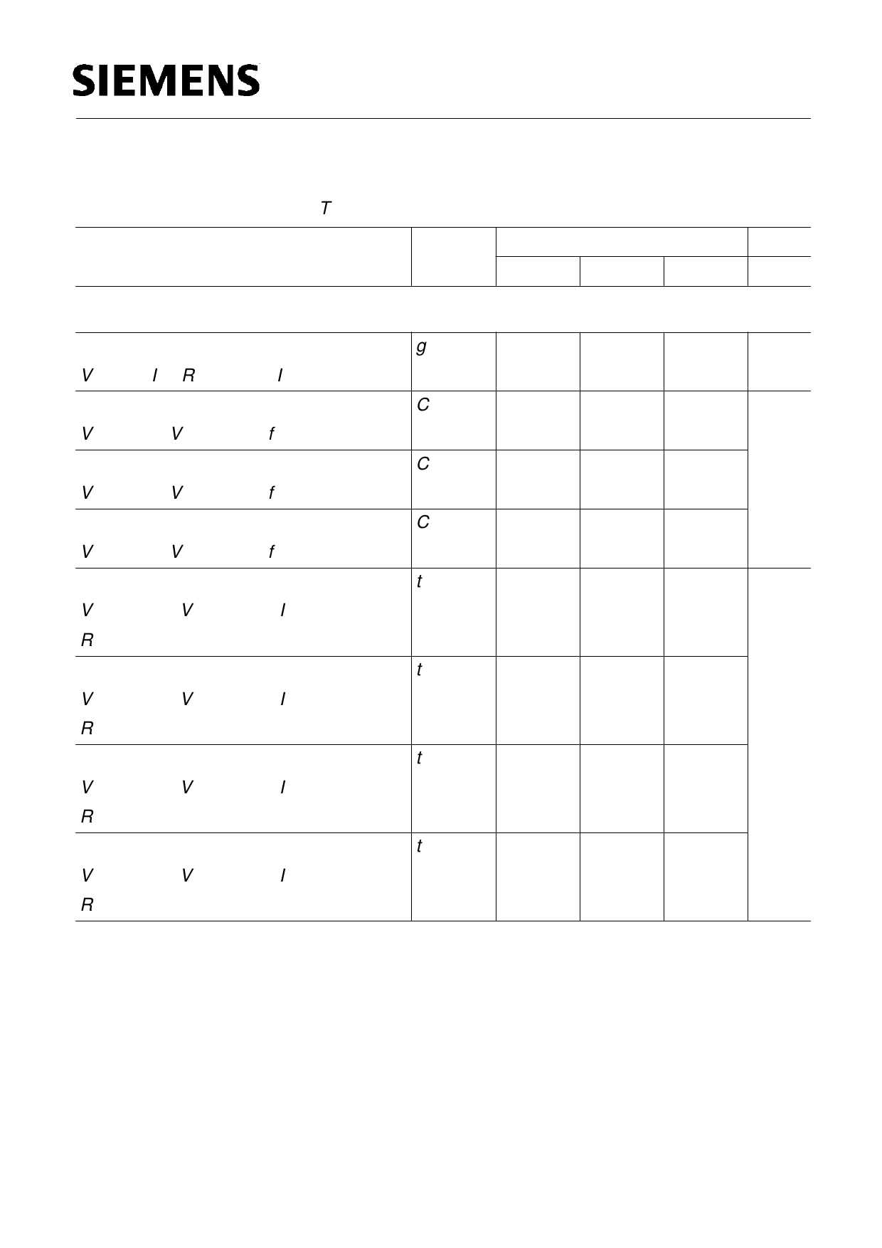
Electrical Characteristics, at Tj = 25°C, unless otherwise specified
Parameter
Symbol
Values
min.
typ.
max.
Dynamic Characteristics
Transconductance
VDS≥ 2 * ID * RDS(on)max, ID = 0.2 A
Input capacitance
VGS = 0 V, VDS = 25 V, f = 1 MHz
Output capacitance
VGS = 0 V, VDS = 25 V, f = 1 MHz
Reverse transfer capacitance
VGS = 0 V, VDS = 25 V, f = 1 MHz
Turn-on delay time
VDD = 30 V, VGS = 10 V, ID = 0.29 A
RGS = 50 Ω
Rise time
VDD = 30 V, VGS = 10 V, ID = 0.29 A
RGS = 50 Ω
Turn-off delay time
VDD = 30 V, VGS = 10 V, ID = 0.29 A
RGS = 50 Ω
Fall time
VDD = 30 V, VGS = 10 V, ID = 0.29 A
RGS = 50 Ω
gfs
0.1
Ciss
-
Coss
-
Crss
-
td(on)
-
tr
-
td(off)
-
tf
-
0.2
-
60
80
15
25
15
25
5
8
5
8
12
16
13
17
Unit
S
pF
ns
Semiconductor Group
3
Sep-13-1996
Share Link: 