CD40192 View Datasheet(PDF) - Intersil
Part Name
Description
MFG CO.
CD40192 Datasheet PDF : 12 Pages
| |||
Specifications CD40192BMS, CD40193BMS
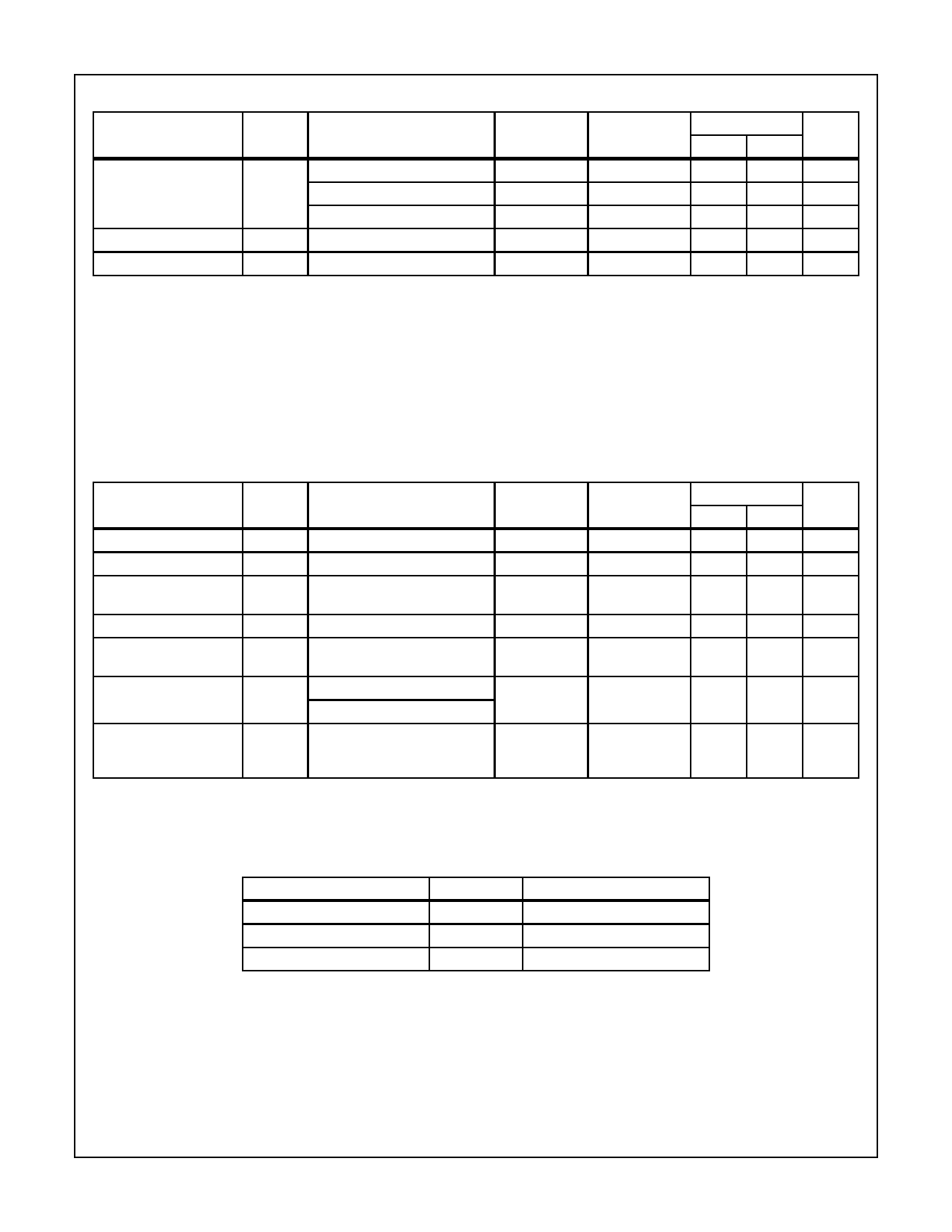
TABLE 3. ELECTRICAL PERFORMANCE CHARACTERISTICS (Continued)
LIMITS
PARAMETER
Minimum Clock Pulse
Width
Input Capacitance
Input Capacitance
SYMBOL
CONDITIONS
TW VDD = 5V
VDD = 10V
VDD = 15V
CIN Reset
CIN All Other Inputs
NOTES
1, 2, 3
1, 2, 3
1, 2, 3
1, 2
1, 2
TEMPERATURE MIN
+25oC
-
+25oC
-
+25oC
-
+25oC
-
+25oC
-
MAX
180
90
60
15
7.5
UNITS
ns
ns
ns
pF
pF
NOTES:
1. All voltages referenced to device GND.
2. The parameters listed on Table 3 are controlled via design or process and are not directly tested. These parameters are characterized on
initial design release and upon design changes which would affect these characteristics.
3. CL = 50pF, RL = 200K, Input TR, TF < 20ns.
4. If more than one unit is cascaded, TRCL should be made less than or equal to the sumof the transition time and the fixed propagation
delay of the output of the driving stage for the estimated capacitive load.
5. The time required for RESET or PRESET ENABLE control to be removed before clocking. See timing diagram defining TREM.
TABLE 4. POST IRRADIATION ELECTRICAL PERFORMANCE CHARACTERISTICS
LIMITS
PARAMETER
Supply Current
N Threshold Voltage
N Threshold Voltage
Delta
P Threshold Voltage
P Threshold Voltage
Delta
Functional
Propagation Delay Time
SYMBOL
CONDITIONS
IDD VDD = 20V, VIN = VDD or GND
VNTH VDD = 10V, ISS = -10µA
∆VTN VDD = 10V, ISS = -10µA
VTP
∆VTP
VSS = 0V, IDD = 10µA
VSS = 0V, IDD = 10µA
F
TPHL
TPLH
VDD = 18V, VIN = VDD or GND
VDD = 3V, VIN = VDD or GND
VDD = 5V
NOTES: 1. All voltages referenced to device GND.
2. CL = 50pF, RL = 200K, Input TR, TF < 20ns.
NOTES
1, 4
1, 4
1, 4
TEMPERATURE MIN
+25oC
-
+25oC
-2.8
+25oC
-
1, 4
+25oC
0.2
1, 4
+25oC
-
1
1, 2, 3, 4
+25oC
+25oC
VOH >
VDD/2
-
3. See Table 2 for +25oC limit.
4. Read and Record
MAX
25
-0.2
±1
2.8
±1
VOL <
VDD/2
1.35 x
+25oC
Limit
UNITS
µA
V
V
V
V
V
ns
TABLE 5. BURN-IN AND LIFE TEST DELTA PARAMETERS +25oC
PARAMETER
SYMBOL
DELTA LIMIT
Supply Current - MSI-2
Output Current (Sink)
Output Current (Source)
IDD
IOL5
IOH5A
± 1.0µA
± 20% x Pre-Test Reading
± 20% x Pre-Test Reading
7-1423
Share Link: 