74LV374D,118 View Datasheet(PDF) - NXP Semiconductors.
Part Name
Description
MFG CO.
74LV374D,118 Datasheet PDF : 17 Pages
| |||
NXP Semiconductors
74LV374
Octal D-type flip-flop; positive edge-trigger; 3-state
VI
CP input
GND
VI
Dn input
GND
VM
tsu
th
VM
tsu
th
Qn output
VOH
VOL
VM
mna202
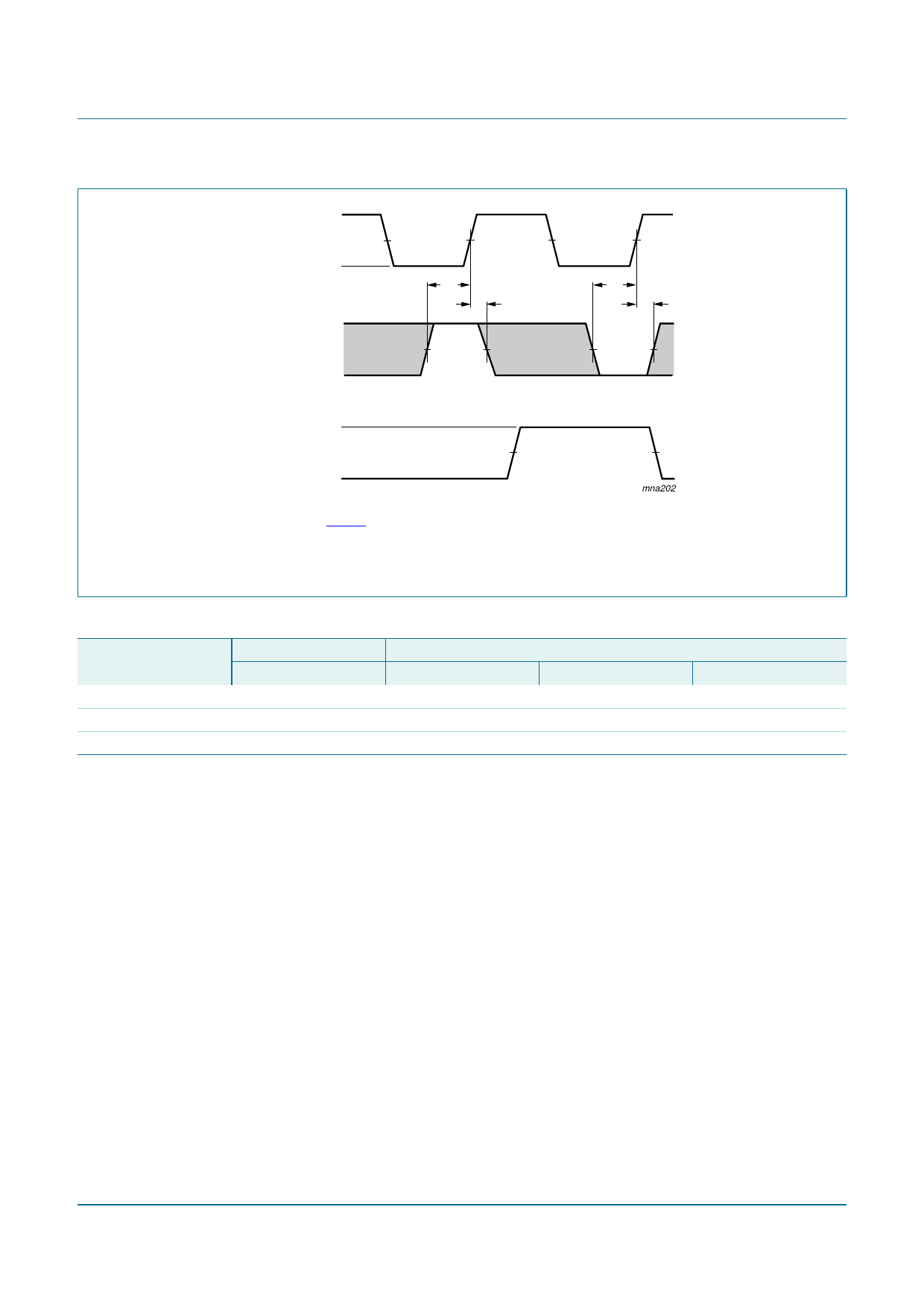
Fig 9.
Measurement points are given in Table 8.
The shaded areas indicate when the input is permitted to change for predictable output performance.
VOL and VOH are typical output voltage levels that occur with the output load.
The data set-up and hold times for the Dn input to the CP input
Table 8. Measurement points
Supply voltage
Input
VCC
< 2.7 V
2.7 V to 3.6 V
VM
0.5VCC
1.5 V
≥ 4.5 V
0.5VCC
Output
VM
0.5VCC
1.5 V
0.5VCC
Vx
VOL + 0.3 V
VOL + 0.3 V
VOL + 0.3 V
Vy
VOH − 0.3 V
VOH − 0.3 V
VOH − 0.3 V
74LV374_2
Product data sheet
Rev. 02 — 14 May 2009
© NXP B.V. 2009. All rights reserved.
9 of 17
Share Link: 