SI7005-B-FM1 View Datasheet(PDF) - Silicon Laboratories
Part Name
Description
MFG CO.
SI7005-B-FM1 Datasheet PDF : 40 Pages
| |||
Si7005
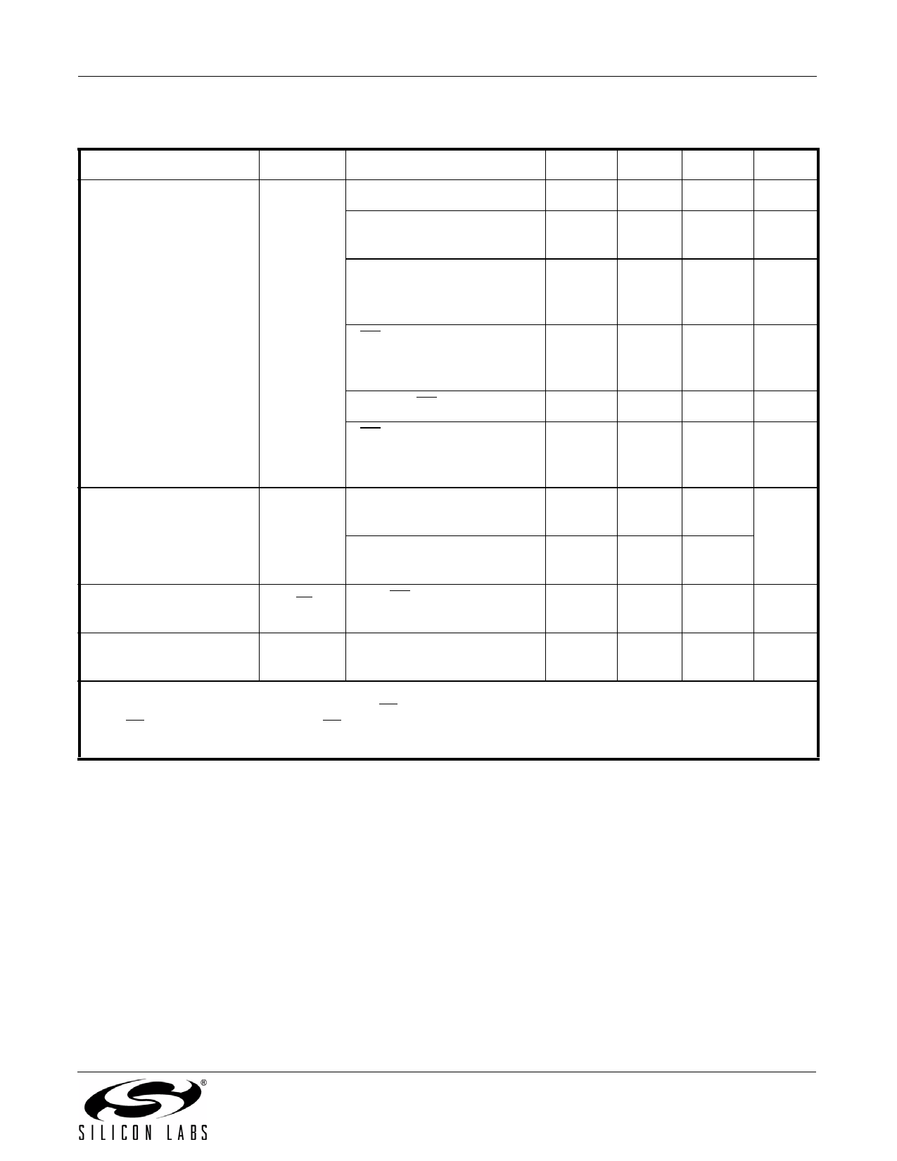
Table 2. General Specifications (Continued)
2.1 VDD 3.6 V; TA = 0 to 70 °C (F grade) or –40 to 85 °C (G grade) unless otherwise noted.
Parameter
Power Consumption
Conversion Time
Wake Up Time
Power Up Time
Symbol
Test Condition
Min
Typ
Max
Unit
IDD
RH conversion in progress
—
240
560
µA
Temperature conversion in
—
320
565
µA
progress
Average for 1 temperature
—
1
—
µA
and 1 RH conversion /
minute
CS < VIL; no conversion in
—
progress; VDD = 3.3 V;
SDA = SCL ≥ VIH
CS > VIH
—
CS < VIL; no conversion in
—
progress; VDD = 3.3 V;
SDA = SCL ≥ VIH; HEAT = 1
tCONV
14-bit temperature; 12-bit RH
(Fast = 0)
13-bit temperature; 11-bit RH
(Fast = 1)
150
—
µA
—
100
µA
24
31
mA
35
40
ms
18
21
tCS
From CS < VIL to ready for a
temp/RH conversion
10
15
ms
tPU
From VDD ≥ 2.1V to ready for
a temp/RH conversion
10
15
ms
Notes:
1. Si7005 can draw excess current if VDD and CS are ramped high together. To enter the lowest power mode, either hold
CS low while VDD ramps or pulse CS low after VDD reaches its final value.
2. SDA and SCL pins have an internal 75 k pull-up resistor to VDD.
Rev. 1.3
5
Share Link: 