74HC283D/AUJ View Datasheet(PDF) - NXP Semiconductors.
Part Name
Description
MFG CO.
74HC283D/AUJ Datasheet PDF : 20 Pages
| |||
Philips Semiconductors
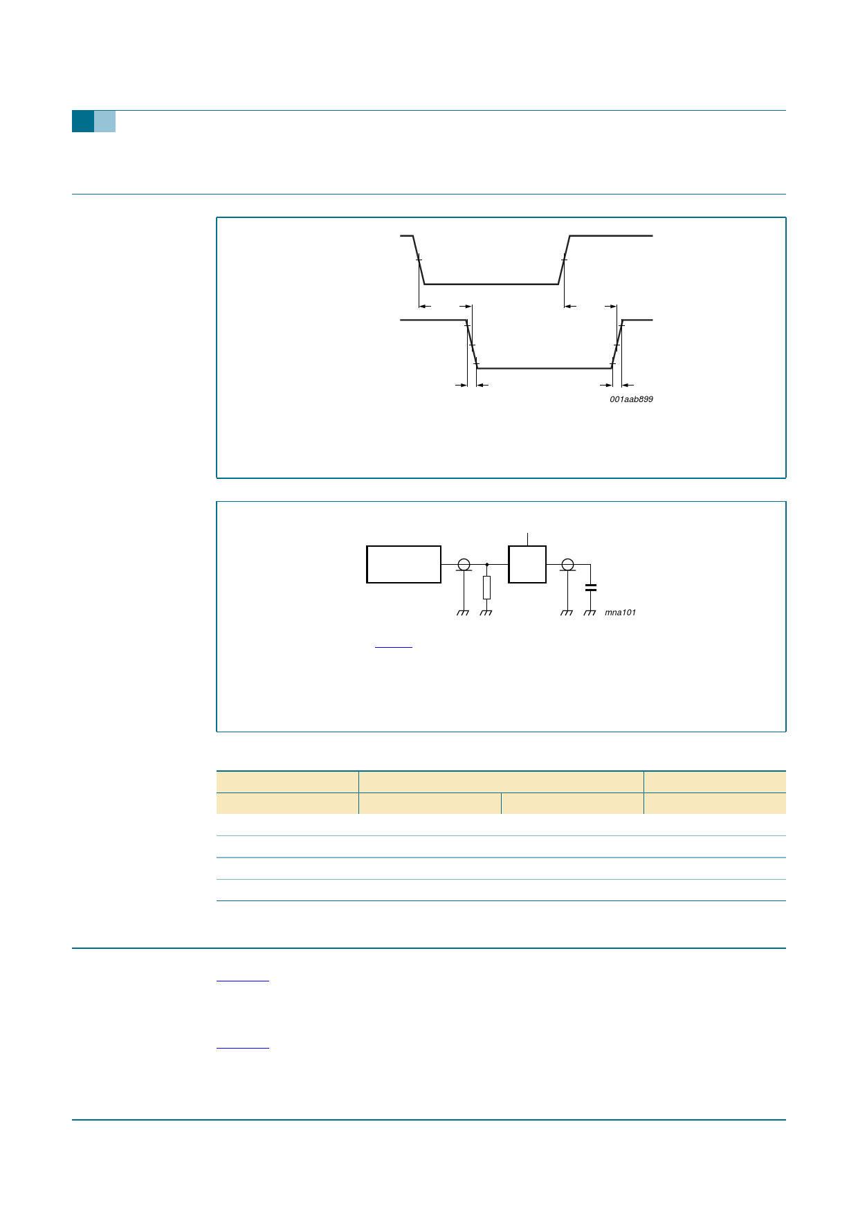
12. Waveforms
74HC283
4-bit binary full adder with fast carry
CIN, An, Bn,
input
VM
Sn, COUT,
output
tPHL
VM
tPLH
tTHL
tTLH
001aab899
VM = 0.5 × VI.
Fig 6. Waveforms showing the inputs (CIN, An and Bn) to the outputs (Sn and COUT)
propagation delays and the output transition times
PULSE
VI
GENERATOR
VCC
VO
D.U.T.
RT
CL
mna101
Fig 7.
Test data is given in Table 9.
Definitions for test circuit:
RT = Termination resistance should be equal to output impedance Zo of the pulse generator.
CL = Load capacitance including jig and probe capacitance.
Load circuitry for switching times
Table 9:
Supply
VCC
2.0 V
4.5 V
6.0 V
5.0 V
Test data
Input
VI
VCC
VCC
VCC
VCC
tr, tf
6 ns
6 ns
6 ns
6 ns
Load
CL
50 pF
50 pF
50 pF
15 pF
13. Application information
Figure 8 shows a 3-bit adder using the 74HC283. Trying the operand inputs of the fourth
adder (A4 and B4) LOW makes S4 dependent on, and equal to, the carry from the third
adder.
Figure 9, based on the same principle, shows a method of dividing the 74HC283 into a
2-bit and 1-bit adder. The third stage adder (A3, B3 and S3) is used simply as means of
transferring the carry into the fourth stage (via A3 and B3) and transferring the carry from
9397 750 13811
Product data sheet
Rev. 03 — 11 November 2004
© Koninklijke Philips Electronics N.V. 2004. All rights reserved.
12 of 20
Share Link: 