74HC191D,652 View Datasheet(PDF) - NXP Semiconductors.
Part Name
Description
MFG CO.
74HC191D,652 Datasheet PDF : 19 Pages
| |||
Nexperia
74HC191
Presettable synchronous 4-bit binary up/down counter
Symbol Parameter Conditions
CPD
power
VI = GND to VCC; VCC = 5 V;
dissipation fi = 1 MHz
capacitance
25 °C
Min Typ Max
[3] - 31 -
-40 °C to +85 °C
Min Max
-
-
-40 °C to +125 °C Unit
Min
Max
-
- pF
[1] tpd is the same as tPHL and tPLH.
[2] tt is the same as tTHL and tTLH.
[3] CPD is used to determine the dynamic power dissipation (PD in μW):
PD = CPD x VCC2 x fi x N + ∑(CL x VCC2 x fo) where:
fi = input frequency in MHz;
fo = output frequency in MHz;
CL = output load capacitance in pF;
VCC = supply voltage in V;
N = number of inputs switching;
∑(CL x VCC2 x fo) = sum of outputs.
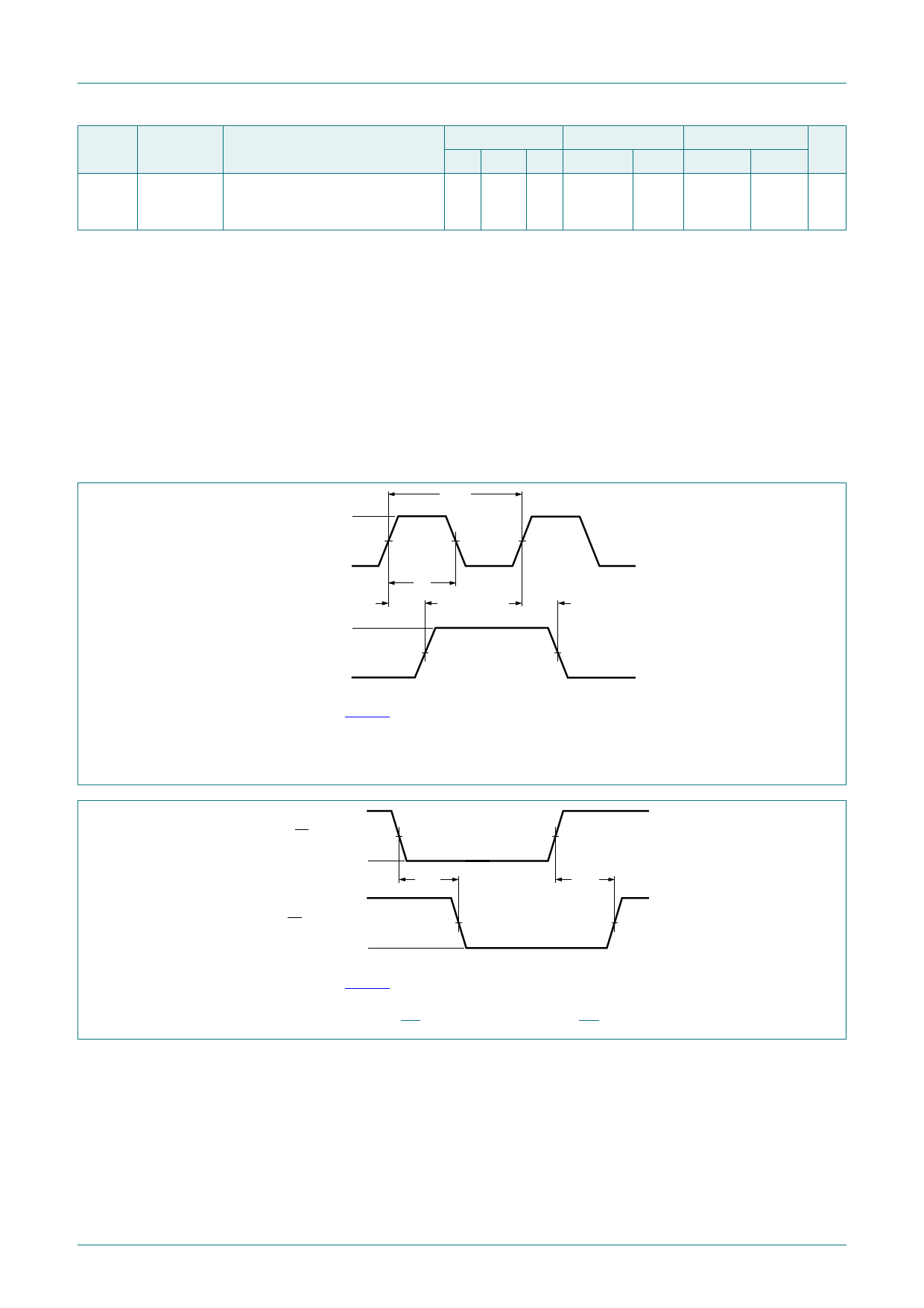
10.1. Waveforms and test circuit
VI
CP input
1/fmax
VM
GND
tW
tPLH
tPHL
VOH
Qn, TC
output
VM
VOL
aaa-024384
Measurement points are given in Table 9.
Logic levels VOL and VOH are typical output voltage levels that occur with the output load.
Fig. 10. The clock input (CP) to outputs (Qn, TC) propagation delays, clock pulse width and maximum clock
frequency
VI
CP, CE input
VM
GND
VOH
tPHL
tPLH
RC output
VM
VOL
aaa-024385
Measurement points are given in Table 9.
Logic levels VOL and VOH are typical output voltage levels that occur with the output load.
Fig. 11. The clock and count enable inputs (CP, CE) to ripple clock output (RC) propagation delays
74HC191
Product data sheet
All information provided in this document is subject to legal disclaimers.
Rev. 4 — 5 October 2018
© Nexperia B.V. 2018. All rights reserved
10 / 18
Share Link: 